The birth of the Soviet missile defense system. The battle of the Soviet ministries for microcircuits
A sharp interest in increasing the level of integration initially came not from the developers of Elbrus-2, but from Przyjalkovsky from NICEVT.
The fact was that, as we have already said, in the mid-1970s there was a real renaissance of ECL BMK. Almost all IBM S/370 clones - Siemens, Fujitsu, Amdahl - moved to custom circuits.
One of the main and, no matter how you say it, good goals of the creation of the EU computers was the constant maintenance of the parity of domestic computers with Western developments.
Naturally, the upcoming Ryad-3 had to be assembled on the same element base in order to keep up with a generation. Przhijalkovsky understood this very well and started a war with the MEP for obtaining new microcircuits (Burtsev pulled himself up later).
The problem was that MEP, who had been tormented to a bloody sweat with the 100/500/700 series, was absolutely not eager to get into the bottle and start a new development, an order of magnitude more difficult than everything they did, having not even really completed the rip off of the previous generation.
As we remember, the mid-70s was the peak of Brezhnev's passivity, a time when ministers preferred to share profitable and problem-free contracts, rather than take on an extra headache.
The most lengthy discussions in the SGC and in NICEVT were conducted on the choice of large integrated circuits.
If the options for using the LSI memory were obvious, then the transfer of the logical structures of the computer to the LIS caused some split among the developers.
For a long time, enterprises in the electronics industry objected to the production of matrix-type LSI. Under the conditions of the existing economic mechanism, it was extremely unprofitable for them to master several hundred types of LSI with a relatively small serial production of each type.
As an alternative, a project was put forward to create a computer on one or several types of microprocessors, microprogrammed to perform the functions of each logic circuit and each node of a large computer.
In these circumstances, with the unwillingness of the electronics industry to produce matrix LSIs and the inability to maintain compatibility not only with IBM, but also with the ES EVM-2 with serious interference in the proven circuitry with microprocessors, a forced decision was made to split the ES EVM-3 into two stages.
The first stage of domestic computers - ES-1036, 1046 and 1066 - to be built on the newest microcircuits of the average degree of integration of the IS-500 series, and the second - EC-1037,1047, 1067 and XNUMX - to be implemented on matrix LSIs, which should have appeared by the time they began design.
Of course, this laid a technological lag behind Western computers, which could not but lead to a lag in architecture, but there was another way out in 1977–1978. did not have.
Przyjalkowski wrote.
It helped, oddly enough, the same damned Afghan war and the arrival of Reagan.
The lethargic dream was abruptly shaken off, the USSR again found itself in the ring of enemies, Reagan joked live on the air:
My compatriots are Americans, I am pleased to inform you today that I signed a decree declaring Russia outlawed forever. The bombing will begin in five minutes.
In general, the glorious times of the maniacs Lemay and MacArthur have practically returned.
The frightened USSR struggled to remember how great infrastructure projects are carried out in general.
Of course, we also had to forget about cooperation with Motorola, no more MC10100 in the ES computers.
IEP is accelerating
In 1979, the MEP urgently began copying the F100K and their BMK F200, while the official public order for the BMK for 1000 valves was formulated a little later, after the program article by Przhiyalkovsky, Lomov and Faizulaev “Problems and ways of technical implementation of high-performance computers based on LSI” , published in USiM No. 6 in 1980.
As a result, the Irbis theme, the cloning of the BMK, got into the plan of the XI five-year plan of 1981–1985, hence the microcircuit indices: I200 (in honor of the F200), I300 (in honor of the F300) and then they wanted to reach their own I400 and I500 (taking for basis is no longer Fairchild).
At the same time, the MEP decided, on the wave of what is called the hype around the second round of the Cold War, to raise the topic of its own supercomputer and begin the development of "Electronics SSBIS", and from the whole breadth of the Russian soul - a family of three machines at once.
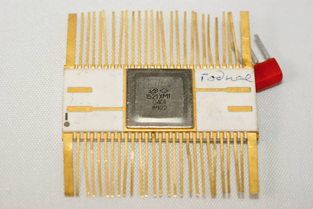
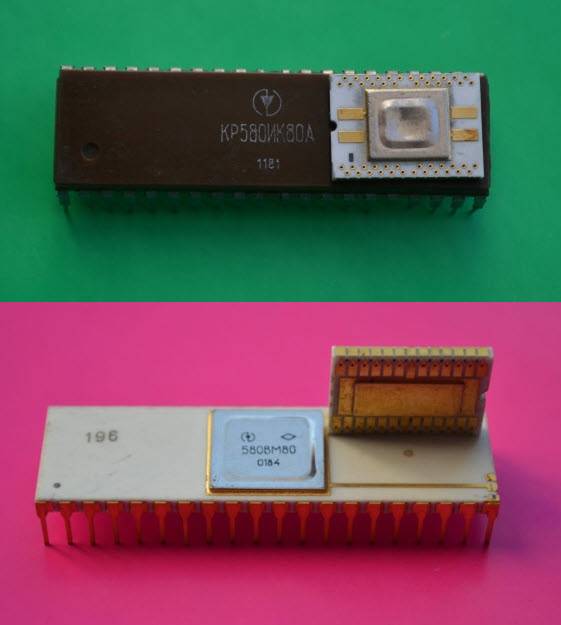
1521XM1 - what the second version of Elbrus-2 was assembled on (photo https://1500py470.livejournal.com)
At the same moment, Burtsev also saw the light and realized that the train of lucrative orders was about to pass ITMiVT directly to NICEVT (and in Ryad-4, Przhiyalkovsky already provided for real supercomputers, plus they were actively sawing the topic of powerful matrix-vector coprocessors for them) and Research Institute "Delta".
Despite the fact that Elbrus-2 on the 100th series has just begun to be debugged, he sharply enters his team into the order list for the 1520th series and at the same time encourages Sokolov to start work on a vector coprocessor for the still not ready Elbrus so that it turns out no worse than that of the MEP.
In addition, by the mid-1980s, he also had an idea for his own line of Elbrus-type supercomputers.
As a result, by 1985, the overworking USSR drags three parallel lines of supercomputers on its hump at once - the potential Elbrus series (3 machines are planned), the potential Elbrus series (3-5 machines are planned) and the potential EU Row 4 series (2-3 machines plus coprocessor projects for them, in addition, they also oversaw completely left-wing architectural developments, such as the Glushkov macro-pipeline, which also received the EU index).
All of them compete fiercely for finance, factories and intellectual resources of developers.
Of all the magnificence, only the second version of Elbrus-2 managed to finish up to small-scale production.
"Electronics SSBIS" (possibly) was made in 4 copies, but none of them was installed and put into operation, after 1991 all machines were handed over for gold.
Row-4 supercomputers were not completed at all.
As we have already said, two projects were launched - the 1500th series (for the F100) and Irbis for the F200.
Microcircuits "Irbis" received the marking K (N) 152x (N - depending on the type of case) and the version XM1-XM6.
The crystals inside these microcircuits were designated as I200 - I500 with different letters, for example, the addition of "B" meant a change in the process technology from 2,5 microns to 1,5 microns.
The 1500th series was primarily intended to replace imports in the older models of the EC Ryad-3 and use in various on-board computers, and was a complete set of various 2I-NE type loose powder, etc.
This series, being newer compared to 100/500/700, was used for the initial development of "Electronics SSBIS" and the EU Row-4.
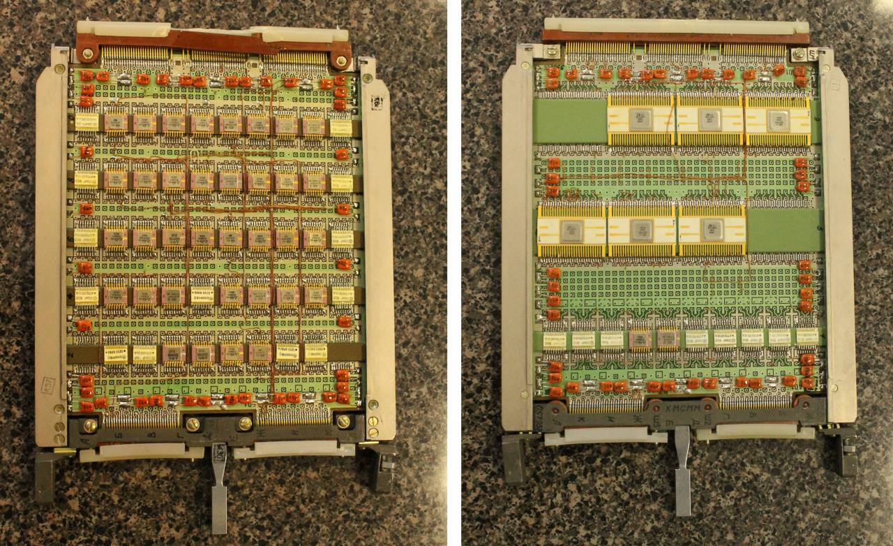
Most likely, the only 2 boards from the Elbrus-2 processor that survived in Russia: one - on the 100th series, the second - on the BMK I200, from the collection of the Siberian Branch of the Russian Academy of Sciences (photo https://1500py470.livejournal.com)
But with the 1520th series, everything was very, very interesting, so much so that the best technoarchaeologists spent several years of research to understand what and how was produced there.
The short version of events is as follows.
The I200 began to be developed in full and sincere agreement between the MEP and MRP, primarily for Elbrus-2, and the crystals of this series became the only ones completely finished and debugged and used in a really working machine that came with them on boards to serial production.
The process took several years, from the beginning of the 1980s to 1985-1986, and the living machine on them was ready approximately by 1987.
It was necessary to complete Elbrus-2 at any cost: both the MEP and the MRP understood this and worked together.
In 1981, the Fairchild F300 BMK series was released, which is eight times more complicated than the F200 and has three power consumption levels: 8, 4 and 2 W, with a speed of 0,4 ns. She was immediately accepted into development as the I300.
Here, as luck would have it, the MEP had already conceived a series of three "Electronics SSBIS", and Burtsev was carried into the vector MCP. Because of this conflict of interest, the MEP Mikron plant began to send representatives of ITMiVT and NITSEVT more and more often on foot trips, so they had to do everything themselves.
As a result, they developed different versions of chips on the I300 in fact in parallel and independently.
Both options were brought to the series, and SSBIS Electronics (final version), Burtsev's MCP and Babayan's Elbrus-3 were assembled on them, but none of these machines really worked.
Further, the MEP team remained to cut the I400 project for the upcoming, in their opinion, "Electronics SSBIS-2" (they wanted to roll it out by 1989, very optimistic, given that they even barely finished the first version by this time), the fate of the I500 is still shrouded in darkness, but it was already the beginning of the 1990s, when Soviet microelectronics ended.
Amusingly, it can be noted that the initial efficiency of the I200 / I300 series (they began to create clones almost earlier than their prototype F200 / F300 officially became available on the civilian market in the United States) is not connected with the Elbrus theme at all, but technoarchaeologists are here like got water in the mouth:
In addition, evil tongues say that the first machine in the USSR on our BMK I200 was not a computer with the letter E (Elbrus and Electronics SS BIS), but a certain machine from the depths of the KBPA, about which I knew nothing at the time, I don’t know now , and I don’t want to know later what I recommend to everyone reading this text.
<...>
It is very likely that our project with the development of Elektronika SS BIS could be a screen for the development and production of a completely different machine, machines or various special equipment, which is still not accepted to talk and write about ...
<...>
It is very likely that our project with the development of Elektronika SS BIS could be a screen for the development and production of a completely different machine, machines or various special equipment, which is still not accepted to talk and write about ...
More than these quotes about potential alternative applications of the I200 is unknown (although, as we remember, in the USA, in parallel with the CDC STAR project, a lot of interesting things were also created).
One way or another, it is reliably known that for the final version of Elbrus-2, KN1520XM1 was used on an I200M 2,5 micron crystal, compatible with the 100/500/700 series.
Initially, KN1521XM1 (I200) was developed, compatible with the 1500 series, but it did not fit for Elbrus-2, since the peripheral cells could not be compatible with both the 100 and 1500 series at once.
In the internal elements of the 1521XM1, the current sources (both in current switches and in emitter followers) are on resistors, which means that when the power rating changes, the resistor rating must also be changed, and the power there was different: 4,5 V and 5,2 V.
In addition, the 100 and 1500 series had different logic levels and different behavior of these levels when the temperature and supply voltage changed. The variant of the crystal on the 1,5 micron process technology, instead of 2,5 microns, was called I200B, and the microcircuit for it was KN1520XM4. On this one they assembled the final version of "Electronics SSBIS".
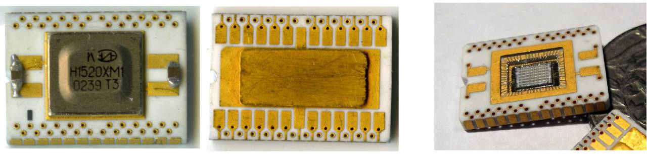
H1520XM1 - the basis of "Electronics SSBIS", and with the cover removed - their almost indistinguishable prototype Fairchild F200 (photo https://1500py470.livejournal.com)
The size of the 1520 series is actually very small. Gold-plated holes are designed for test probes and duplicate pads (photo https://1500py470.livejournal.com)
According to the memoirs of Elbrus-2 engineers:
1521XM1 matches the dimensions and wiring with the K200, so that you can simply mechanically solder them.
The performance is about 2 times faster.
The exception is memory.
The 1521 had no memory on the chip, only logic, so a direct replacement for the K200 with cache was impossible.
The cache memory boards were redesigned, each microassembly with 8 700RU148 chips (64 bits) was replaced by two 100RU410A chips (256 bits), while the new board (regular, without microassemblies) became half empty, a lot of free seats.
Nevertheless, these boards (both densely packed, all the seats on both sides are occupied on K200, and half-empty on 100RU410A) were exact functional analogues, one was replaced by another, often in one processor there were TECs of both varieties.
100RU410A was released later than 100RU148, so it was impossible to immediately make it on 100RU410A.
They have been made since about 1985, when Elbrus-2 was being tested in 1984. They were not there yet.
Each HM1 was heated by 4 W, as a result, more than 0,5 kW had to be removed from one TEC.
Elbrus-2 managed with water-cooling on a water-alcohol mixture (like the MCP), but the monstrous and 2 times more powerful Electronics SSBIS required freon.
It was the only machine in the USSR with cryogenic cooling (although, again, there were rumors about some top-secret projects with cooling at a phase transition - nitrogen evaporation), and they suffered enough with it.
The development of BMK for Elbrus-2 was completed in 1983–1984, and the first processor was assembled on them in 1986, but it did not work.
It took the MEP a few more years to master the production of the I200 at the proper level, and the same number of ITMiVT to create suitable TEZs for them.
The first versions of "Elbrus" at the BMK were inoperable, as the academicians screwed up the cooling system, there were no specialists of the level of Cray among them.
The first XM1 ceramic cases simply cracked as a result of heating, as the mounted cooling was insufficient.
There was also a problem with the hulls, the first batches had to be purchased in Japan, since the plant in Yoshkar-Ola experienced numerous difficulties with their development.
One way or another, the first 100% operational Elbrus-2 of the second generation was introduced only in 1989.
The problem was not only with cases, for the manufacture of working ICs from blanks-BMK, appropriate CAD systems are needed, doing it by hand is a completely thankless task.
The Moloch-type hull for the KH1500 series was the Mizula-type hull rugs for the 1520th. On these, perhaps, the first version of "Electronics SSBIS" was assembled (photo https://1500py470.livejournal.com)
We should also say a word about Soviet RAM chips for high-performance systems.
Memory in a supercomputer is the third most important thing, after a processor and a cooling system (and competent cooling design generally comes first, which our high-browed theorists, who are accustomed to developing computers by drawing multi-colored squares, “and here we plump super- mega processor).
When in the summer of 1980 the first TOR was approved for research work on the SSBIS, ours focused on Cyber 203 and CRAY-1. Memory of 1 megaword seemed quite decent, and everyone expected that as a result it would be necessary to make RAM with an access time of 60–80 ns, 64 bits plus control, sufficient to correct single errors and detect double ones.
The task to start copying the F100K series was sent to three organizations, NIIME, Integral and Svetlana, back in February 1980 with a requirement to complete no later than December 1981.
Due to the importance of the task, the first microcircuit of the series, K1500RU415, was simultaneously covered by NIIME and Integral. At the same time, in parallel with the plant in Yoshkar-Ola, they were instructed to develop a flatpack-24 case.
However, either the development of the flatpack was not mastered, or such a package did not pull out the desired frequency (due to the inductance of the outputs), but as a result, a completely different package was developed at the plant in Donskoy as soon as possible, an analogue of the American cerpack-24, to establish the production of an experimental batch of the 1500th memory was only possible by 1982, and the series - even later.

Progress in RAM for 10 years 1990 to 2000. 1 server plate per 64 MB = 1024 TEZ from Elektronika SSBIS. RAM rack. It weighs three tons, consumes 22,5 kW, requires an additional freon cooling rack SOH-32, power rack and 1/2 water cooling rack BOX-20 to remove heat from the power supply. The photo shows in sequence a RAM rack, a freon refrigerator for it, food, water cooling of food. In total, the counter ate about 25 cubic meters of water per hour (photo https://1500py470.livejournal.com)
Minsk Integral was instructed to develop a TEZ for this economy (ROC "Desant-1" and "Desant-2").
The first pancake came out lumpy, TEZs had a monstrous temperature gradient and mercilessly failed.
I had to develop a second version of the board and carry out a preliminary sorting of the IC at low temperatures of minus 15-30 degrees, so that you could quickly identify failed copies. This required the development of a new measurement setup and climatic chambers.
At the NICEVT, at the same time, they suffered with the same problems.
As a result, the MTBF for the rack was still about 20 hours.
By the summer of 1986, they still finished off three memory racks, however, one TEZ was not half enough.
When, under the project "Electronics SS BIS-2", they decided to increase the RAM by 8 times, they opened a new R & D "Desant-3" for the K1500RU470 microcircuits, but it all ended in nothing.
How to design a microchip?
With the design of the machine, the situation is generally extremely difficult.
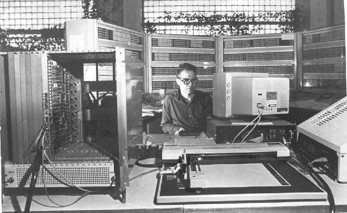
Probably the last Hi-End computer that used manual methods was the Cray-1.
As we wrote in a previous article, Cray was a genius for minimalism, which made it easier for him and his team to work.
He assembled the entire logic of the supercomputer on a single logical element, dual 4OR / 5OR-NOT, which made it possible to express the architecture in the form of a series of generally recognized logical formulas (and not like Lebedev's own esoteric language).
As a result, his employees simply carefully transferred Cray's notes to real chips. All this splendor was mounted on a five-layer board, in which only the top 2 layers were signal, and the bottom three were solid: -5,2 V, -2 V and ground. Two such boards were folded like a sandwich on a sheet of copper, through which heat was removed, and sent to the rack.
The thermal package and power consumption were calculated by equalizing the number of cases on the board, because all the elements were the same. This automatically resulted in equal heat dissipation and power consumption for the racks.
Race conditions were fought effectively, simply due to the same length of all twisted-pair interconnects.
In fact, the Cray-1 was purely architecturally simple to disgrace, and this made it possible to finish the car with a record-breaking small team and carefully assemble it without the slightest jambs, moreover, in terms of performance, it did everything that was in the world at that moment.
Compare: only by 1989 it was hardly caught up with the monstrously bulky and complex Elbrus-2, with which a crowd of people was transported for 20 years, despite the fact that the Cray-1 loader was so simple that old Seymour remembered it by heart.
Unfortunately, except for Yuditsky and Kartsev (whose machines, as we remember, worked effectively even on a terrible Soviet element base, without requiring to fool around with the BMK), Soviet designers of the "academic" direction did not understand the ideas of architectural simplicity and purity at all.
Sockets for mounting microcircuits in one of the options "Electronics SSBIS" (photo https://1500py470.livejournal.com)
From the point of view of Soviet scientific research institutes, the more difficult - the cooler, therefore, in the end, the same "Electronics SSBIS" was described by its developers themselves (already much later, when it became possible) as follows:
The UVC of our design had access to 576 contacts, which is four of 144. So I remember from my stove.
By today's standards, the size of the printed circuit board is larger than the size of a cool laptop!
I don't remember the power supply. Probably, as on Elbrus, the sources were planned under a raised floor.
In my opinion, the design of the SS LSI was a pretentious g ... m unjustified decisions. One nonsense of freon cooling was worth something.
But everything was very solid and academic and occupied half the stadium, not a couple of rooms, and gave out (in theory) only twice as much Cray-1.
For the Cray-1 itself, engineers calmly and quickly spread 113 types of printed circuit boards with their hands, which made it possible to lay the development in 1972-1976.
The car was built with the expectation of subsequent upgrades, and already in Rev. D used 23 types of IC and four times more capacious memory.
In fact, every six months (until 1985) a new iteration was released, using a cheaper, more technologically advanced and modern element base, so the Cray-1 of the first and last releases are in reality different machines.
In 1972, only 12 people worked on the supercomputer - the entire staff of Cray Research, by 1976 there were 24 of them. Only when mass production began, they had to hire about a hundred installers and engineers.

The monstrous processor board "Electronics SSBIS", the panels UK48-1 and UK52-1 for KN1520XM4 and copper pipes for freon cooling are visible (photo https://1500py470.livejournal.com)
Even when the CDC6600 came out, an extremely upset Thomas Watson Jr., director of IBM, called his employees together and asked:
Last week Control Data had a press conference during which they officially announced their 6600 system. I understand that in the laboratory developing this system there are only 34 people, "including the janitor". Of these, 14 are engineers and 4 are programmers, and only one person has a Ph.D., a relatively junior programmer. To the outsider, the laboratory appeared to cost conscious, hardworking and highly motivated.
Contrasting this modest effort with our own vast development activities, I fail to understand why we have lost our industry leadership position by letting someone else offer the world's most powerful computer. At Jenny Lake, I think top priority should be given to a discussion as to what we are doing wrong and how we should go about changing it immediately.
Contrasting this modest effort with our own vast development activities, I fail to understand why we have lost our industry leadership position by letting someone else offer the world's most powerful computer. At Jenny Lake, I think top priority should be given to a discussion as to what we are doing wrong and how we should go about changing it immediately.
Hearing about this stories, Cray sarcastically replied:
It seems like Mr. Watson has answered his own question.
Nevertheless, by 1980 it became clear that with the current rate of growth in the complexity of the BMC, it was no longer an option to spread them with your hands, CAD was needed.
In principle, they have been used in the West, although not massively, since 1967-1968. (In particular, IBM used its own generation environment to develop the S/370 BMK project). Fairchild thought about these by the mid-1970s and released them with the F100/F200.
Designing a completely new computer (well, or cloning an old one, but, as in the case of Elbrus, with a generous admixture of “improvements”) consists of the following steps.
First, a system of commands is developed (the so-called ISA, the only thing Lebedev could do, and even then BESM-6 turned out to be a bit of techno-schizophrenia).
Next - we need to put the command system on a real crystal. The first step is the translation of ISA into the language of logic circuits. In the West, as a rule, they use VHDL, SystemC or System Verilog for this, most of these tools appeared in the early 1980s and were unknown in the USSR.
Cray, due to the simplicity of Cray-1, did the translation by hand (Lebedev in BESM-6 also invented his own unreadable notation in which he described the entire architecture of the machine), Fairchild developed its own design environment for working with the F100 / F200 back in the mid-1970s (it collected CDC CYBER of all versions). Many companies such as Fujitsu, IBM and Siemens offered their own proprietary systems.
It is this stage that is responsible for ensuring that the chip generally does what it needs.
Then comes the stage of designing the physical circuit.
At this stage, the logic we implemented is tried on for a specific BMC. This means that we need to generate a physical circuit based on its description, perform clock synthesis, routing, etc.
Physical design doesn't affect functionality at all (if done right), but it does determine how fast the chip runs and how much it costs.
At this stage, numerous patented algorithms for the optimal placement of logic elements on a chip, often developed by manufacturers of the BMC themselves, can be used. Naturally, the result obtained needs tests and verification, which is often the most difficult process.
The first efficient test synthesis algorithm was developed by John Paul Roth of IBM only in 1966. Actually, all Soviet testing algorithms were its copy or generalizations.
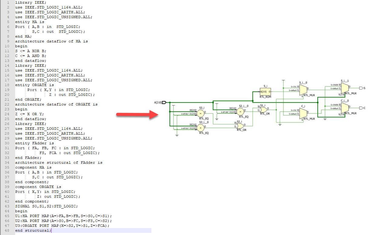
One of the most primitive adder options on VHDL, description and synthesis
When we synthesized one crystal in this way, the procedure must be repeated for all the basic chips from which the machine will be assembled - to synthesize all the logic, registers, control device, etc. in crystals.
As soon as all this is placed on the BMK (well, or in parallel with this), they begin to design printed circuit boards for them. It is necessary to determine their size, the number of layers, separate the power supply and buses, place crystals on them. In order to route the boards and verify the result, their own CAD systems are also used.
In parallel with the synthesis of boards, a construct for them and power and cooling systems are being developed.
Thus, all cars of the 1970-1980s were created.
In the USSR, computer-aided design methods began to develop at about the same time as in the United States - in the mid-1960s.
Almost everything that is known about early Soviet developments fits in one paragraph of Malashevich:
In 1964, I. Ya. Landau proposed the language for modeling logic circuits FOROS. In 1965, G. G. Ryabov at ITMiVT began the development of CAD, later called PULSE, and N. Ya. Matyukhin headed the work on computer design automation. In 1967, O.N. Yurin began to deal with the issues of CAD computers, who in the 70s headed the development of CAD ESAP (Unified System for Automation of Design) at NICEVT. In Kiev, V. M. Glushkov and colleagues are developing the fundamental questions of computer design automation.
Nothing reliable could be found either about FOROS or I. Ya.
Nevertheless, it is reliably known that this PULSE lasted in service until the mid-1980s, it worked exclusively on BESM-6 and was inconvenient to use.
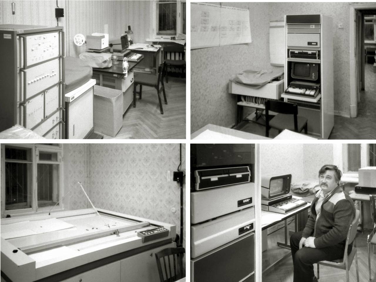
D. E. Guryev, who worked at Delta on the 22nd floor with their CAD zoo, recalls:
In the Research Institute "Delta", in the department of Melnikov, there really was a CAD department, which was led by my teacher Yaitskov Alexander Sergeevich. And this department developed its own CAD. Not PULSE. PULSE was also (stolen?!), and all the logic design of the I200 / I300 / I300B crystals was performed on it.
But the development / maintenance of this product was handled by someone else, not from our department.
Our CAD was focused on design engineering. And not only microchips, but also boards in which they should be installed.
The work of our system began with the import of a logic diagram from PULSE: a list of elements and their interconnections, which, as I understand it, is called the word NETLIST in Western CAD systems.
Both PULSE and our CAD were run on BESM-6. She had all the peripherals already from the ES computer. This machine was controlled using the Dispak OS, MS Dubna, the JIN dialog system were also used.
Our CAD also had its own means of managing the computational process, developed within the department, in particular, a specialized job control language and a file system (even three).
Our development was carried out in the Pascal language on the compiler of A. S. Pirin.
CAD carried out the tracing of electrical circuits for blocks and microcircuits.
This set of algorithms was developed by Vladimir Susov and his small team.
The placement of elements seemed to be manual or semi-automatic. In any case, I do not remember the full automation of this design stage.
CAD provided the output of design results to the media necessary for production processes. (I don’t know the details of the implementation, except for those with which I was personally involved, more on that below.)
Personally, I was busy developing a subsystem that synthesized output and input control tests for I200/I300/I300B. I had pre-processing, organization of the computational process, post-processing, analytics and optimizing transformations.
In short, I did almost all the dirty work in this subsystem.
In addition to the main algorithm, which was directly handled by A. S. Yaitskov and his wife G. A. Yaitskova.
The system resulted in texts in the input language of the Centry testing system used at the plant in Zelenograd.
They were recorded on magnetic tape at BESM and then, lo and behold, they were read by this bourgeois equipment and executed by it.
To write to tape, I had to dig deeper into the low-level commands for controlling the tape drive.
There was also an interface wrapping the synthesized tests back into PULSE, and there they were used as additional design verification tests, modeled by PULSE, of course. Several mistakes of chip designers were revealed on these tests.
An important part of our CAD was the delay verification algorithms, both at the level of chip designs and at the level of board designs.
At a given frequency, the length of the conductors is already a factor affecting the speed of signal propagation and, thus, the correct operation of the digital circuit as a whole.
The algorithms evaluated the correctness of the topology design in terms of delay propagation and signaled where the design was at risk and what needed to be fixed. A. S. Yaitskov and Tatyana Ganzha were engaged in these algorithms.
CAD used two separate file systems: for CAD source texts and for initial, intermediate, and output design data.
Both systems were developed by Vladimir Safonov.
An alternative FS for design data was developed by Vladimir Susov.
Here it is necessary to explain to the modern reader that DISPAK OS had neither a standard file system, nor a standard text editor, or a standard task management language, and all these tasks were solved in their own way in each major applied project.
The SAP did not have a name. After all, the name is needed for a product that will be delivered somewhere. Nothing of the sort was planned here.
CAD supported the current project. The part related to the construction of tests was referred to as "CAD Test" in several scientific articles, but this was a name only for the context of these articles.
I came in 1984.
By that time, the department existed, as I understand it, for about 5 years, and there were already working tracing algorithms.
Work on testware began already in my memory, around 1985, work on verification of delays a little later.
I left in 1990.
The department continued for two more years.
After that, its already small fragments were transferred to the ISP and existed there for another 5 years.

CAD PULSE and how it was used to model micro-BESM from Dubna's brochure "Logical modeling of the MKB-8601 processor"
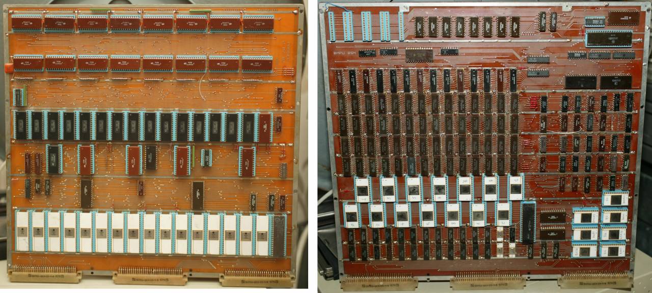
As a result, the development for BMK I200 / I300 was carried out by the following systems. CAD BASKY (basic automated control and manufacturing system) on BESM-6, 29 schemes were developed on I200, 25 of which were made in silicon.
BASKY received input data from PULSE and gave the result to TOPTRAN, consisted of 300 thousand lines of Pascal code. SAPRB (blocks) served for the development of TEZ, worked similarly on BESM-6 and took into account when designing signal delays between elements on the PCB and between blocks.
SPIN (interactive design system) was created to transfer the documentation developed at the Delta Research Institute to industry enterprises, it was formed under Electronics 100–25 and 79. Its main function was to translate the software project from SAPRB into an understandable for NPO Quartz CAD format PENDANT.
For completeness of happiness - none of these systems were graphic!
No, there were no graphics.
And there were no such devices.
It was then that I looked at foreign CADs - it turns out that this is primarily a graphic editor, and then algorithms.
And we had algorithms without a kin. For the issuance of graphic materials necessary for the production of boards, there was a contact with a friendly organization (or an allied company) in the city of Chernogolovka. They had the right equipment.
Yes, we had display stations, but they were alphanumeric terminals.
The work of CAD programmers and hardware engineers was conditionally interactive. But it was work with signs.
The same PULSE is a means of writing formulas that specify the operation of a device (or its model), which is called RTL in modern CAD systems.
There were no graphics due to the lack of suitable devices as a class.
There were only output graphic devices for preparing technological data for production, and even then, I remember, they were rented.
The launch of a certain task: compiling a program, modeling a circuit, performing some design operation (for example, tracing conductors), went through the general task queue of the system, in which, in fact, electronic images of punched cards were located, and these tasks were performed in batch mode (as if they would actually come in the form of a deck of cards).
Western CAD, which appeared in our country in the late 80s on personal computers, professed a completely different principle: it is, first of all, a graphic editor, to which some kind of automation of individual design operations can be connected, or maybe not.
For us, automatic algorithms worked, but without graphics and with limited human participation.
The person gave the task in text form, in it he also evaluated the result, if he didn’t like it, he changed the task, and started his virtual deck of punched cards on a new one.
However, it seemed that there was a control language, like a shell, but much simpler, which helped to partially automate this process, but the results of the work of such shell commands or shell programs were still launching virtual decks of punched cards.
Printed circuit board topology layout in Zelenograd. It was in this marvelous place that the SPIN design automation system worked, which was engaged in the translation of output files from CADB and BASKY into files understandable for other CAD systems at other MEP enterprises (photo https://1500py470.livejournal.com)
ITMiVT used the no less mystical KOMPAS-82 system (and, again, everyone has no idea if it has anything to do with the modern Compass).
She worked on top of PULSE and in conjunction with it, of course, on the ideologically correct BESM-6, which by the standards of the 1980s was already a living nightmare.
PULSE, by the way, was also noted in Dubna - in the late 1980s they developed their own version of micro-BESM on microcircuits (MKB-8601, 4 boards of about 100 microcircuits), but no one needed it.
Of the interesting architectural features of PULSE, it can be noted that it was written purely under the DISPACK OS and nothing else, so the JINR engineers had to tinker a lot.
Portability was absent as a class, since more than 300 DISPACK extracodes of 20+ types were hardcoded in PULSE, and the system itself was distributed by its authors in the form of a library of load modules, so making changes to it yourself required preliminary detranslation of modules into autocode, now such a procedure would be called disassembly .
As a result, the dispakov's crutches were sawn out and replaced with DUBNA OS subroutines. The four-month fuss was not in vain - the system accelerated twice.
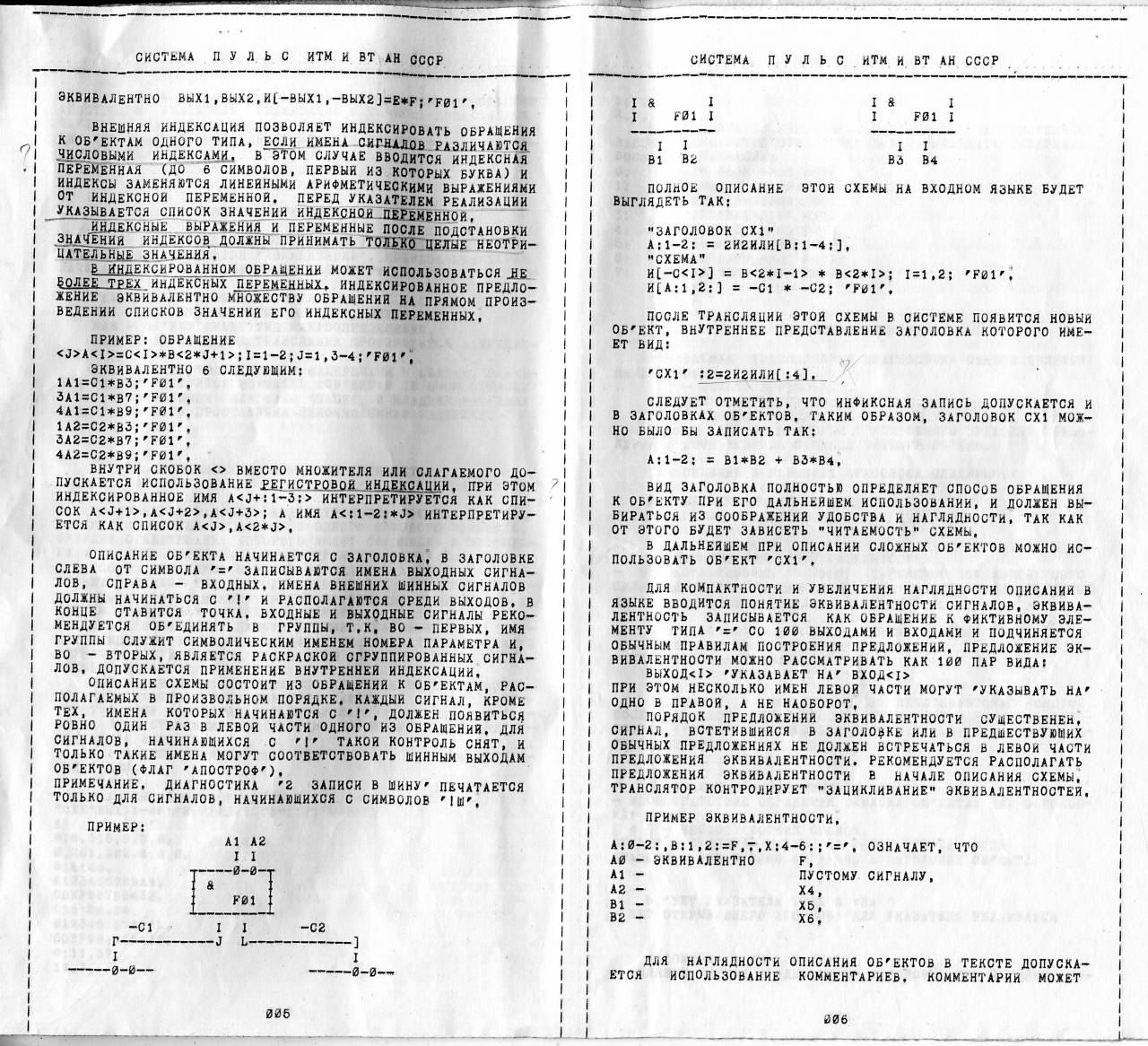
Instructions for PULSE. Terrible documentation quality.
By 1987, the 14th version of PULSE was already released, but whether it became the last one or not is unknown.
In the mid-80s, corresponding member V.P. Ivannikov became interested in the VHDL language and took a number of steps to implement it in Delta. Under his leadership was a group developing a compiler (and probably a simulation system) for VHDL.
As a result, we wrote a converter from PULSE to VHDL, and that was it.
The same Micro-BESM, the last one designed in PULSE (photo https://ruecm.forum2x2.ru)
And her unique boards: the only thing that survived from 2 copies (photo http://www.nedopc.org)
Distinguished, of course, NICEVT. They worked there, obviously, for the EU. Under it was its own native CAD - EASP, which was used for Row-4.
In the mid-1980s, NICEVT showed itself to be the most progressive organization in general.
Firstly, they licensed the European BMK Siemens SH100 for cloning (and turned them into 1520XM5, more on that below), and secondly, along with the crystals, they got the Siemens AULIS proprietary CAD system.
The problem was that AULIS was originally developed under the BS2000 OS, which ran on the German analogue S/370 Siemens P1 (and more advanced ones). This line was not a development of a pure S / 360, but the same as the British, its clone RCA Spectra 70, modified and not compatible with our EU.
The question arises - did NICEVT also buy a German mainframe?
Or rewritten CAD for the EU?
In theory, it could also be launched on the M-4000.
This is the only S / 360 clone that NICEVT had nothing to do with at all, it was even ripped off from a completely different machine - just the same Siemens 4004, and they did it in the former Brukovsky INEUM that we have already forgotten in 1972-1977. On it, BS2000, in theory, could start natively or with minimal finishing. In the early 1980s, there were several dozen M-4000s in Moscow, they could use one of them.
As a result, when NICEVT nevertheless mastered AULIS in the mid-1980s, it is reliably known that the process of designing a crystal was reduced from 2 weeks (NII Delta, pure PULSE) or 4–5 days (ITMiVT, KOMPAS- 82) up to one working day.
Riddles of the Soviet XM1-XM6 series
The design problem was exacerbated by the choice of prototype.
The MEP copied almost simultaneously MCA600ECL for ITMiVT, where they generated 1521XM1, MCA1200ECL for NICEVT, where 1521XM2 and 4.101VZh3 were presented to the world, and F200K Gate Array, which gave birth to KH1520XM1.
Later, only BMKs compatible with the 1500 series were developed.
Naturally, such a number of parallel projects could not but affect their quality and timing.
The picture was further aggravated by the fact that, judging by the datasheets, 1521XM1 was a bit of a Frankenstein compilation of offal MCA600ECL and peripherals from Fairchild FGE.
It is funny that in 1993 Burtsev (when it became possible) separately walked through the Soviet system in his memorandum about Elbrus-2 in the Russian Academy of Sciences:
The element base ... was produced in a country with a monopoly on the production of integrated circuits (IEP), therefore, it has a probability of failure not of 10-8–10-9 degrees, as in foreign countries, but only 10-6–10-7. This suggests that the schemes have not been fully mastered to date.
Again, this is 1993!
And our schemes are not fully mastered.
However, as we have already said, all this mess around the development led to the fact that in the end the project failed, everyone (except Babayan and Ryabov) managed to get a hat, and the remaining years of their lives, using freedom of speech, explained their attitude towards each other .
"Electronics SSBIS" also experienced a change in the element base, in general, people from "Delta" began to dig into the topic with the BMK back in the 1979 region (which gave rise to rumors that the MEP magnum opus was a cover for another top secret military project, although about We know enough about Elbrus, and it would seem that it is much more secret than the machine of the anti-missile shield of our homeland).
As a result, they toiled terribly with the I200 trace, using every conceivable means from bare hands (at first) to PULSE.
After long and varied experiments, heaps of broken crystals and non-working prototype boards, according to the memoirs of veterans:
... the idea of raising the BMK to 3 valves, except by hand, was alien to Zelenograd hero workers.
But something based on the I200 nevertheless began to emerge, although after 1981 it was decided to use the more advanced I300 - a clone of the Fairchild F300 series FGE2000 (for 2 valves).
This is how the K1520XM3 microcircuits (I300b crystal) appeared, already exclusively for the MEP.
The second iteration went more fun, in 1984 there were not even cases for them, but by 1985 the prototype "Electronics SSBIS" was put up for testing.
It was at this moment that both Przyjalkovsky and Burtsev received their first thrashing from the MEP.
Przyjalkowski recalls:
In 1983, having made sure that the Zelenograd plant "Mikron" could not or did not want to produce for NICEVT matrix LSI I-300, the only LSI on which it was possible to create an older model of the ES computer, the management of NICEVT suggested that the director of "Mikron" supply basic crystals, and the tracing of the two upper layers of the crystal, packaging and output control to take over, along with responsibility for the LSI as a whole.
At the same time, it was possible to convince the Minister of Radio Industry P. S. Pleshakov that the building of the MCI technical college with an area of 21 thousand square meters. m, the construction of which was completed by the Ministry with the help of NICEVT at the NICEVT site, it is advisable to re-profil it for the development and production of special LSI for MCI, including matrix ones.
Having received the consent of the minister, the management of NICEVT staffed a new complex department and, with the help of the ministry, equipped it, having mastered new areas.
By the beginning of 1985, despite the insufficiently developed technology and the low quality of the basic crystals supplied from the MEP, the first working matrix LSIs of the I-300 series began to appear at NITsEVT.
In 1984, the efforts of the NITSEVT were crowned with success, they independently designed, packaged and manufactured the first IC on the I300b, installed it as an experiment in the EU-1066, and it started up!
The IS received a temporary index 4.101VZh3 and was a functional analogue of the Melnikovskaya KN1520XM3.
In all likelihood, they again had to purchase test batch cases from the Japanese (who in those years tried to expand their market, suffocated by Reagan, at the expense of the Union and began to slowly spit on KoK, Toshiba secretly drove the USSR to the USSR with its precision machines for processing submarine propellers).
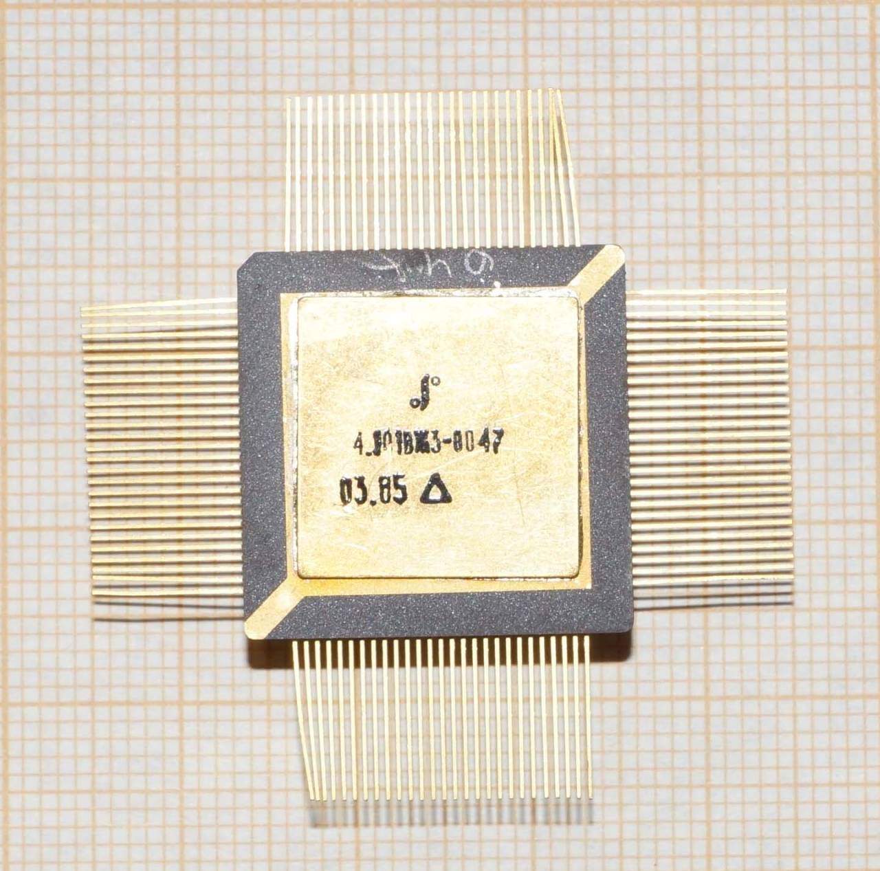
Chip 4.101VZh3 developed and manufactured by NICEVT, made on I300, an analogue of Melnikovsky XM3, was used in prototypes of Ryad-4 supercars and MCP Burtsev. Also on it, most likely, they made a prototype of Elbrus-3. It was marked like this, and not (K) the XM series number, the development number, in order to circumvent the MEP monopoly on the production of microcircuits (photo https://1500py470.livejournal.com)
NICEVT generously shared what was made with ITMiVT, moreover, their development teams sat together on Varshavka in the premises of the third complex department of NICEVT.
The crystal was fiddled with for quite some time, until the late 1980s, the original version was prone to self-excitation of the input stages on the parasitic reactances of the outputs. In fact, only a few test batches were made, which went to no less trial machines.
As a result, the technology obviously lagged behind by 8–9 years, turning already assembled prototypes into a pumpkin.

Gorgeous photo of the I300 crystal and its fragments (photo https://1500py470.livejournal.com)
An interesting fact is that the same legendary building at that moment was in a state of continuous completion (and in the end it was never completed in its intended form).
Denis Rodomin, a specialist in Soviet architecture, says:
The project was created by the architect Vsevolod Voznesensky back in 1969, construction began in 1972.
The house in the form of a large arc was supposed to become part of a large complex of scientific institutions.
It was planned to build a tower in the center of this ensemble.
But in the end, only a “lying skyscraper” and two more architectural arcs closer to the Moscow Ring Road were born.
The project of the scientific campus did not receive proper funding: atypical structures required special attention and large funds.
As a result, some elements of the building had to be created using truly artisanal methods, and construction was delayed.
The house was commissioned only in the late 80s.
Inside, it was noticeably different from the original project.
An even sadder fate befell their competitors from the MEP.
No longer lying, but quite a traditional skyscraper - a monument to Shokin's sense of greatness.
In 1967, the architect Novikov proposed to build two towers for the MEP, 24 and 20 floors high, the project was repeatedly reworked, postponed and began to be implemented in a truncated form only in 1985, and by 1991 they had only managed to finish the cladding.
As a result, the unfinished building was purchased by Lukoil for its headquarters, turning it into one of the ugliest buildings in Moscow.
It's also funny that with the third competitor - Research Institute "Delta", about the same story happened, but they were the luckiest of all, well, their father, the Design Bureau of Semiconductor Engineering (KBPM), was very fat and secret.
There is no information about them on Wikipedia and almost nothing is known at all.
It was formed already in 1961 and was engaged in the "development and production of special equipment for the assembly of semiconductor devices" - that's all we know about them.
Since 1978, it has specialized in special communications, including fiber optic systems.
In 1977, the “Organization of PO Box 3390” stood out from them, about which there is also little information, except that it is a semiconductor engineering laboratory at the KBPM, which received the civilian name of the Delta Research Institute.
It was in this secret trench coat of Elbrus that Melnikov and his team went.
Delta Headquarters, a modernist skyscraper on Shchelkovskoye Highway, began to be built in 1971 according to a Japanese project, extremely unusual in everything, including the internal layout.
Alas, the Japanese project did not want to stand on Russian soil and began to roll, which was successfully hidden by adding 2 more smaller volumes to the side.
It was erected epic, from 1971 to 1983, and in a still unfinished building and worked on "Electronics SSBIS".
By the way, the same "Delta" was engaged in microcircuits, not just military ones, of the 5th acceptance, but even of the 9th - products of a special grade, used only in spy satellites, and the Kremlin's special communications.
On the roof (unprecedented for the USSR) a helipad was installed!
In 1983, the research institute's field of activity was expanded by the scientific division for fiber optic technology, which in 1984 was transformed into an independent institution.
In 1986, the Delta NPO was created, which included, in addition to the research institutes, their Elling plant and the Disk plant in the Oryol region.
The SSBIS Electronics project was personally supervised by Deputy Minister Kolesnikov, and the director of Delta was, in general, Shokin's son.
Melnikov, too, could not be given the directorship, and he headed the Institute for Cybernetics Problems of the USSR Academy of Sciences, created in 1983, where he dragged his friend and colleague on the AS-6 project V.P. Ivannikov, who once worked on the very first and dense OS for BESM -6 - D-68.
Theoretically, the IPK was supposed to focus on the development of software for "Electronics SSBIS", in practice, the elderly academics were doing their favorite thing - intrigues and the development of funds.
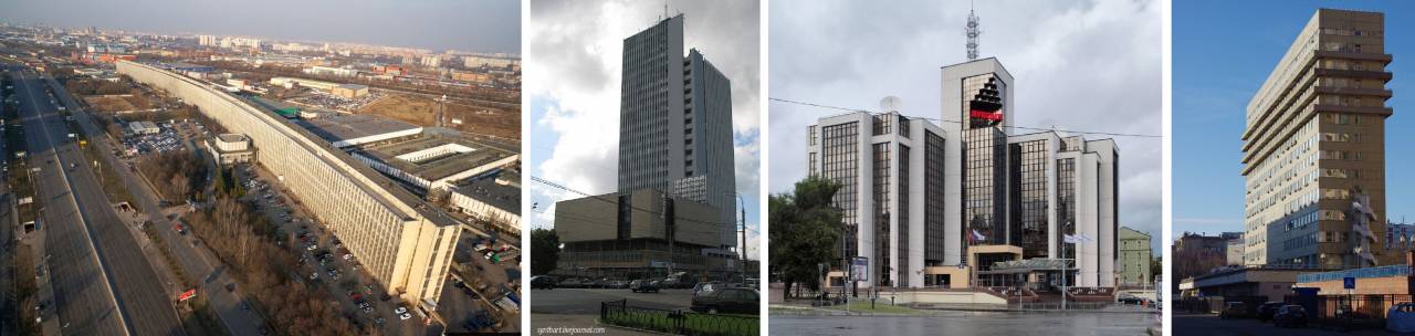
Ruins of a more advanced civilization. The building of the NICEVT on Varshavskoe shosse, the tower of the Research Institute "Delta", the headquarters of the MEP, which was never completed under the USSR, and the building of the IPK of the USSR Academy of Sciences in Cheryomushki. It was planned to put in the Delta tower and the IPK building each piece of SSBIS Electronics (photo https://ru.wikipedia.org, https://synthart.livejournal.com, https://stroi.mos.ru)
One of the participants of those events recalls:
Somewhere in 1987-1988, our initiative group at the Physicotechnical Institute took up SS BIS at the suggestion of Oleg Batsukov.
As it turned out later, in a year a team of about six people produced more software than the entire Ivannikovsky Institute for System Programming in a five-year period.
Made C compiler, assembler, linker. Simulator, mathematical libraries.
As a result, Ivannikov took Vitya Yanitsky to his graduate school, tried to lure others.
I visited them, spoke with the developers of the operating system.
But the impression was rotten, and I lost interest in the project.
By the way, the IPM did not manage to master the OS SSBIS, as well as to write at least something working for it.
But in 1984, Ivannikov was elected a corresponding member of the USSR Academy of Sciences, and after the death of Melnikov in 1993, he headed the Institute for System Programming (ISP) of the Russian Academy of Sciences, created on the basis of the IPK.
The IPK building (now occupied by NIISI RAS) was also “lucky”.
It was built in the legendary Novye Cheryomushki district, where they planned to build an entire academic campus, starting from the building of the largest House of Books in the world and ending with a bunch of research institutes along Nakhimovsky Prospekt.
However, the same curse of the 1980s played - almost nothing was completed (the House of the Book was built according to the American project for the Olympics, but with the outbreak of the Afghan war, the construction stopped, and it was completed only in the late 1990s).
By 1991, the IPK building was half completed (despite the fact that according to the documents it was 100% - it had no decoration, elevators did not work, etc.), and all overspending was generously included in the budget of SSBIS Electronics.
Despite the fact that NIISI RAS is now adorned with a proud sign “Academician Melnikov worked here,” he practically did not appear in the most unfinished building.
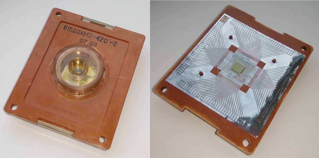
A mysterious artifact of NPO ELAS, a frameless version 1520XM2, obviously for space purposes. I300S is written on the crystal. What it is, why, etc. - is unknown in principle. One of the techno-archaeologists claimed that this was used at one of the Kharkov instrument-making plants for the control machine of something cosmic. These ICs were located on ceramic boards approximately 15x15 cm in size. B1019EM1-2 was also mandatory on each board. The microcircuits of the B1500, 822TsNRXX series also served as the element base. Each such large hybrid was not individually sealed, a general sealing of the entire machine was used. In general, in the USSR there were often series for one specific customer (https://1500py470.livejournal.com)
Given all this, it is not surprising that the rumors about the top-secret Delta projects, for which Electronics SSBIS served as a disguise, as well as the fact that until 1991 it received virtually unlimited funding, surpassing even Elbrus-2.
The secrecy, surpassing even the missile defense systems (after all, some developments were obviously made here for the Politburo itself, including special communications), is also understandable, as well as why the MEP clung so stubbornly to Elektronika to the end.
In general, the history of Delta is incredibly muddy.
Here is what one of those who tried to unearth the topic with the creation of "Electronics SSBIS" said about this:
Many people worked on that project, and those ASs had many authors, but there are many questions about them, the painful similarity to the IBM patent to the point of confusion, that is, the person’s recollection that he was supposedly in charge of such and such a system, but he is not in the list of authors, or already adults who have become accomplished specialists, and the source of their pride is that they have implemented a certain function in the SS LIS, but then the joke begins in general, they are not in the list of authors in the AU, and describe at least in words, but how it was done, they cannot, the designers, who not only cannot say on which series of microcircuits the LSI SS was made, but also poke a finger at the samples of microcircuits laid out on the table, etc., etc.
You probably can’t even imagine the reaction of people when they start talking to them on this topic with documents and artifacts in their hands.
<...>
Yes, then it was a fairly common practice to include in the list of authors who were not involved and exclude those responsible for the creation.
But you need to take into account that in those lists there are people from simple engineers to academicians, touchy at that...
It is very likely that this story is not just hushed up ...
Curious information for reflection, I search websites with resumes and when I find a person who is looking for a job with a line about participation in the BIS CC project, I call, out of 12 people I talked to as a potential employer, only 2,5 people were sane , and then you realize with horror that Gurkovsky is most likely right, and not out of anger says that when he came to the Delta in 81, there was a crowd that was 20 years behind the current level at that time, imagine my sincere trauma when talking to people stuck in the 60s with BESM-6 and fashionable youth devices like ASP-6 and Bull computers in their heads, and stories that they wanted to tell in secret, how NITSEVT destroyed the Soviet VT!
And yes, they are offended by life, that their merits are not appreciated, they cannot find a job, etc.
<...>
And yes, I completely forgot, the sources are divided into three types, the vast majority of those who position themselves as the creators of the SS LSI do not understand anything at all, it is not clear how they could work, the remaining smaller part is quoted by me verbatim, but their attitude to the matter can be seen from the quotes, the minority the overwhelming type of Gurkovsky literally in a few minutes is ready to break into obscene words when talking about what was happening ...
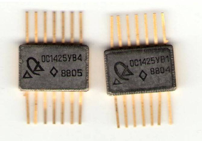
One of the results of the work of the Research Institute "Delta" - microcircuits of special grade
One of the few adequate memories of the Delta Research Institute came from a person who just did not work in Melnikov's group:
From what I remember.
It was the first department (and the department where I worked was both the second and the third).
The first was the first in importance (prestige, salaries of employees, location in our tower on Schelkovskoye Highway, 2, in my opinion, and the total number of employees too, but I’m not entirely sure about the latter).
I do not rule out that the Melnikovites also had other sites.
In any case, all sorts of priorities were much higher for them. Their paramount importance has always been declared.
In other words, it was felt that Melnikov & Co is a state within a state.
It was not customary to go to them.
Something like that.
My close associates and I were (and still are) analog people, while everyone there is digital…
There wasn't much interest.
I only remember that “all THIS” got very hot there (there were, apparently, problems with power dissipation).
And they also made their calculations on BESM-6, of which they had plenty of good, and they worked well, did not hang (unlike our super-buggy EU-1060, which was quickly replaced by the viable GDR ES-1055M, on which, however, , there was the ever-memorable PELICAN, which was an adapted version of SPICE2.G6.
I also remember that there were rumors that the very name "Delta" means a kind of triumvirate, where the main peak is the Melnikovites, and we would have to make microcircuits for them, and one more peak along the line of Shokin A. A. (optical communication channels) .
Maybe that's how it was intended, at least bureaucratically, and sounds, in any case, formally logical.
Nevertheless, we did not make any microcircuits for them, we pulled our old webbing.
Now it is clear why, by 1985, Mikron and the MEP finally sent everyone on a long journey, except for the Melnikov group, as a result, all other developments of the MRP were carried out, in fact, independently (and there was nothing for this by the MEP - again, evaluate the thickness of the blat, if he overrides even the military developments of the nuclear shield of the USSR).
At the same time, the record amount ever paid by the MEP for the purchase of production is also understandable - for Elektronika SSBIS, an entire French plant for the manufacture of printed circuit boards was purchased for $ 100 million (MRP also bought a factory for itself, but thinner - for only 70 million).
As a result, the MRP ended with the fact that a group of designers from the third branch of the EITCEVT was taken to a separate NPO "Physics".
NICEVT had to sharply catch up with IBM.
Their 3081 used a processor in the MCM form factor, on a BMC of their own design. Its analogue, the flagship of Ryad-3, ES-1066, was assembled only on the K500 - a small loose powder.
That's what they were going to do in the framework of Row-4.
The first prototype was the EU-1087 - the same as the EU-1066, but the TEZ on the K500 is replaced by one BMK on the I300b.
In fact, it was a draft of the series, like Elbrus-1 for Elbrus-2.
One experimental computer was built from 1985 to 1988. The delays in production were understandable - it was required to transfer 230 types of TEC to the BMC, which resulted in about 50 man-years of work (12 people x 2 months at the TEC in the BMC x 4 years).
The design of BMK tracing, as in Zelenograd, was mainly done by hand, verification was automated. Crystals on the I200 were not suitable for such work - the TEZ did not fit into 1 valves, and therefore we had to develop the topology on the I000b ourselves.
In total, 3 machines were physically manufactured on this crystal - EC-1087, EC-1091 (later renamed 1181, even later - 1187) and 1195.
The EC-1181 was supposed to become a serial embodiment of the EC-1087, as a result, exactly 1 demonstration machine was also assembled in 1989, and the SKB of the Minsk Plant had to be involved in the development, which transferred the channel processor to the BMK.
The EC-1187 was supposed to be the first EC to be completely transferred to the BMK, a processor on one TEZ of 4 ICs. In the EU-1087, they planned to make only a processor on the BMK, and take everything else from the EU-1066.
Due to the fact that the car was made two years longer than planned, by the time it was completed, no one needed it.
According to the recollections of the participants, NICEVT invested most of its efforts in fundamentally new developments of three machines, and with the EU-1087 they hoped that it would somehow work out on its own, but, alas, it turned out as always.
As a result, the EU-1187 was formally completed in a single copy, along with the same single “supercomputer” (because there was only one name left from super by that year) EU-1195 - only by 1995, simply by purchasing the BMK from IBM, since after 1991 there were no problems with it.
Both cars were not needed by anyone for obvious reasons.
They also planned to manufacture the EU-1191 supercomputer, but work on it was stopped in 1989.
As a result, despite the heroic efforts of the chip developers, work on Row-4 in Moscow was completely failed.
In principle, it was not the fault of the people from NICEVT - they simply did not have enough time, skills and technology. 20 years of systematic work in cooperation with IBM - and the result would have appeared, but there was no such time and such opportunities.
Two more Row-4 cars were made outside of Moscow.
ES-1170 was developed in Yerevan without any success until the collapse of the USSR.
The EC-1130 was developed in Minsk with the participation of specialists from Moscow and Kiev on the basis of another clone - a 4-bit BSP Motorola. With us, it has turned into a K1800 microprocessor section. The section itself was developed absolutely independently of the capital's showdowns in 1979 in the Vilnius Design Bureau and completed a few years later. Integration of up to 1 elements, clock frequency up to 000 MHz. Since the developers were as far away from Moscow as possible, the result was achieved, the car went into series, becoming the last Soviet serial EU and the only one from Series-36 that was actually used. A total of 4 computers were made.
The old storyteller Babayan, as always, could not resist the incredible tales:
We won a competition with NICEVT, which at the time was copying non-superscalar IBM machines. We compared it with two machines ES-1060 (an old machine similar to IBM/3033) and EC-1066 (the newest NICEVT machine at that time, analogous to IBM/3081). We surpassed the first by 10 times, and the second by 2 times on the single-processor Elbrus-2, and on the dual-processor Elbrus-2 - 5 times. It was not competition with NICEVT, but with IBM, since they made exact (clock precise) copies of IBM machines, and we had one technological base.
The designer of the same EU-1066 (and the subsequent Series-4), and not a storyteller, Yuri Sergeevich Lomov indignantly objects:
The EC 1066 has many of the mechanisms of superscalar computers: a pipeline for eight stations (stages), several execution units for parallel execution of instructions, branch prediction with simultaneous buffering of three instruction streams, dynamic address translation technology, fast address translation buffers, i.e. address cache, remaining still scalar.
The Elbrus 2 architecture is a superscalar. This architecture was known much earlier than Elbrus was created. It was used by the CDC and Burroughs corporations. This architecture was also used by IBM in the IBM 360/91 model back in the mid-1960s.
This does not mean that all the problems of this architecture have been solved.
The use of a superscalar not only narrows the range of use of general-purpose computers, transferring it from the zone of a universal class to a specialized one, but also requires significant additional equipment, increases the cost and power consumption, and therefore was not used in the ES computer project.
In 1972, after simulating the superscalar of the IBM 360/91 CPU, we already knew that the mechanism that allowed the permutation of operations was still very complex. With five or six arithmetic devices, he did not slow down, and when they became 10-15-20, he was already choking.
We also knew that it was not only the number of arithmetic units that was the issue, but the limitations of the SISD architecture. With the development of the structure of computers of this architecture, the determining factors leading to the disruption of the flow of commands and data become the determining factors, in this regard, the influence of such parameters as the logical dependence of commands, interruptions, branching, conflict, mutual influence of request processing levels, distribution strategy executive resources and management strategy.
The superscalar chokes when the logical dependence of commands reaches 5–6. If in the 1960s the use of this architecture was justified by the requirements of such monsters as Los Alamos and NASA, who were ready for any costs to solve their problems, then by the 1980s the SISD architecture had exhausted itself, and other methods began to achieve high performance.
And those statements that the superscalar architecture was not used abroad because they thought of it there only in 1995 are, at least, cunning.
Indeed, at this time, Intel implemented the superscalar in the microprocessor. Thus, he did not invent, but immortalized the final result of the development of the SISD architecture, one of the greatest achievements of human thought. Made it public domain and available for further wide and reasonable use.
The performance of the IBM 3083 (single-processor version), according to the most conservative estimates, is 1,35 times higher than Elbrus 2 and 3 times higher than the EU 1066.
Checked on the famous problem from Arzamas.
The time to solve it for EU 1066 is 14,5 hours (the act of state tests).
The time to solve it on Elbrus 2 is 7,25 hours, while the IBM 3083 should solve this problem in 3,2 hours, that is, 2,24 times faster.
In addition, IBM 3083 has one rack, EC 1066 has 3 racks, and Elbrus 2 has 6 racks (the central part is taken for all machines).
IBM's result was achieved primarily due to 4th generation technologies. But an even greater role was played by a creative reasonable attitude to development.
The developers faced a dilemma: either two full processors in two racks, each of which was one-third empty. This would make it possible to obtain the maximum possible performance of a two-processor model. Or fill this empty space.
But what?
They came up with a processor without memory - an attached processor - and received in 2 racks 4 (IBM 3084), and in one rack 2 processor version (IBM 3081), albeit with a slightly reduced performance, in relation to the two-rack version .
But by placing a 2-processor variant in 4 racks, they made up for the losses of the single-rack variant.
Under what microscope did Babayan see an exact copy (clock precise) of IBM 1066 in EU 3081?
The result was disappointing, Lomov recalls again:
The transition to the element base of the fourth generation was accompanied by some crisis caused by matrix LSI, the only thing that was at our disposal.
Matrix LSIs did not fit CISC structures well and allowed designing according to the so-called random logic (when the structure is cut into matrix blanks without any scientific justification).
Foreign countries came out of this situation in different ways.
At that time, for example, the RISC architecture appeared, which is less critical to the use of matrix LSIs.
Several fourth-generation machines have already been developed abroad: the 470 and 580 series by Amdahl, the M200H computer by Hitachi, and the 4300 series computer by IBM.
In these LSI computers, various types of structures were used: cassette (4300 and M200H series computers), planar (470 series computers), stacked (580 series computers).
By that time, our technologies made it possible to implement these types of structures.
But we took the path of minimizing the numerous problems when designing on matrix LSIs and developed the technology of the EC1087-EC1181 line, the fourth generation models.
IBM in the IBM 3080 series models, on the contrary, went for an unprecedented complication of technology, rightly believing that there is only one correct way out of the problems that have arisen - the creation of LSI with meaningful regular logic, i.e. microprocessors.
How many years IBM has been working on this technology is unknown, but if we started such a development, it is now known for sure that we would finish it when no one needed it.
And they took a step in this direction by developing a complex intermediate structure - the TCM100 (Thermal Conduction Module) ceramic module.
The whole technological complexity consisted in special ceramics with 33 layers, where 118 bare chips (flipchips) were placed, each of which contained 121 contacts.
The module was connected to the next level of construction using 1 ball leads. This level had 800 pins that were bonded (flipchips montage) to the TCM36 modules.
The TCM100 modules were water cooled.
No one in the world has been able to replicate this technology. With it, IBM outperformed us so much that even with the most sophisticated technology that we were then capable of, we still would not have achieved such performance.
This was followed by the most esoteric variants of the BMK, about each of which almost nothing is known.
BMK 1520XM5 (I-DN series, but this is not accurate) contains 8 integrated elements (transistors and resistors) or 900 equivalent gates, as well as a random access memory (RAM) with a capacity of 650 bits with a tunable organization and an address access time of 512 ns . Made using isoplanar technology.
That, in fact, is all that we know about her, and the reliability of this information is unknown.
It is only clear that the XM5 has once again changed the prototype - it became the Siemens SH100G Gate Array (apparently, the European clone of the F100) along with something called LSI124. Together with the ITMiVT crystal, we received from Siemens their AULIS CAD system for BMK wiring, which made it possible to increase the design efficiency several times.
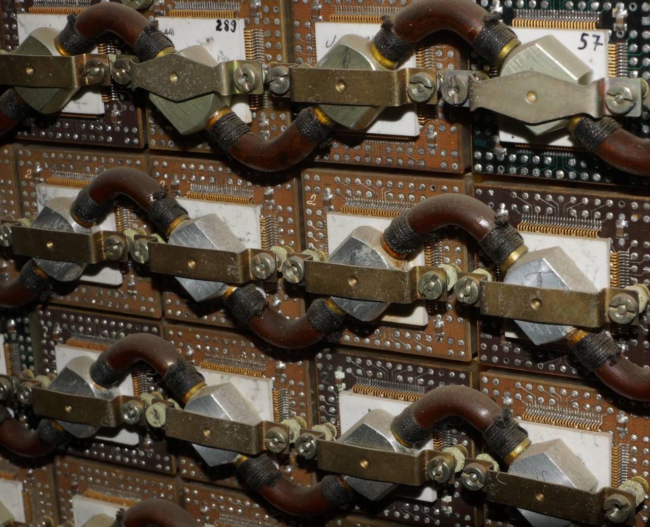
MCP processor cooling (aka Sokolov's Elbrus-3.1), photo from the Polytechnic Museum in Moscow. On the microcircuit board with I300 crystals (photo https://1500py470.livejournal.com)
The BMK K1520XM6 was already being developed again at Delta for the hypothetical Elektronika SSBIS-2, it was supposed to contain 10 valves.
The crystal was called I400 (I400b?).
The chip itself reliably exists, and collectors have seen it, but there is also little information:
As we saw on the slides about SS BIS 2, some hitherto unseen BMK I400B appears.
Unfortunately, it is undated.
Before him, I only came across references to the I400.
When he showed up, science does not know exactly, but in 1986 the guys who had an internship at the NICEVT told in a whisper that we have such devices, but we won’t tell you about them, and spoke with inspiration about the romance of working with I400 ballasts, on which tin melts.
A ballast is an empty microcircuit case in which there is a heating element equal in power to the future microcircuit, they are needed in order to work out the design of REA boards and cases, power supplies and cooling systems even before it is released by production.
In addition, from people who were engaged in the summer of 86 with a subsystem of mass semiconductor memory for already SS LSI 2, they managed to learn very interesting things.
Two variants of the implementation of a parallel algorithm for decoding (80,64)-code on matrix LSIs I200B and I400 are considered.
The first version of the decoding device consists of 32 I200B LSIs of two types, while the encoding device is implemented on 8 I200B LSIs.
The second version of the device is implemented on two BIS I400.
The decoding time is 10 logical levels in the first variant and 8 logical levels in the second variant.
The coding time is 6 levels for the first option, 4 levels for the second.
Devices for encoding and decoding the composite (80,64)-code are located in the UDVP for each access line of the RAM.
In Nefedov's monumental 12-volume book, you can find out that its case is already a typical PGA and formal parameters, that's actually all ...
There is even less information about the mythical I500 for "Electronics SSBIS3".
Only the contents of a pair of slides are known about this machine, created for the report of the JIHTA RAS commission on the preparation of proposals in the field of computer technology in 1991 and first published at the conference in 2018.
There are some very, very hypothetical I500 30K gates with 0,15 ns delays on the slide, but everyone very much doubts that their development has even begun.
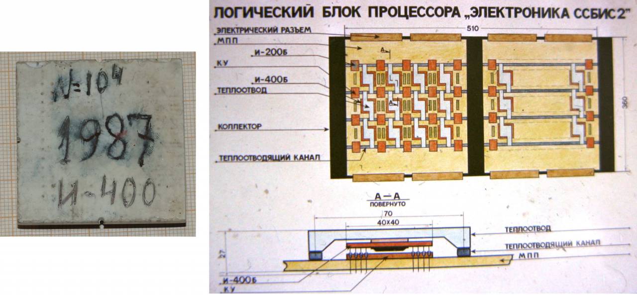
The only known photo of the mysterious I400 and the sweet dreams of academicians about the SSBIS series, for which it is so good to receive endless funding (photo https://1500py470.livejournal.com)
The year 1991 was generally a turning point for the Academy.
Monstrous state funding of useless and insane projects, on which academicians raised money for decades, and the honors abruptly ended, and they began to desperately get out, advertising to the new government no less crazy projects of all sorts of "Electronics SSBIS-2" and 3, failing to start even the first one properly.
The new government was in no hurry to allocate money for slides with "brilliant" architecture, described in the form of multi-colored boxes with arrows "and here we will put a super mega-intelligent processor", the new government was in no hurry, so the fuse was wasted.
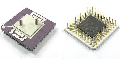
Siemens SH100G Gate Array, from which 1520XM5 was made (I-DN crystal), we do not know its purpose
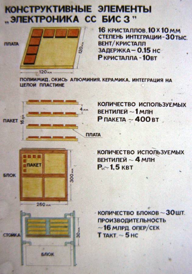
No less sweet dreams about "Electronics SSBIS-3" on the I500 crystal (photo https://1500py470.livejournal.com)[
A typical high-tech production in the USSR, starting from Brezhnev's coming to power, looked something like this (from memories from Habr one of the developersthat spent the entire 1980s in the space industry):
In OKB Fakel, where I designed the plasma-ion engine, the work was built through bureaucratic rituals, and in the field of technical competence - through the ass ...
At the Research Institute of Physical Measurements, the top is a absurd caudle with links to the shadow economy. To protect themselves, they blocked the promotion of bright capable people to the top.
And for example, in the 80s, NIIFI every year took up the development of its CMOS microcircuits. And each time it ended in failure.
I remember that I also twitched to develop my own microcircuit, filled out a bunch of bureaucratic paperwork, and eventually received funding ... when suddenly everyone got into this money and divided it up.
The management gave the project itself to Mikhail Fedorovich, exactly the shot that, according to CMOS, has so far failed everything.
And by the end of this epic I was forced (as a workhorse) to write a report on the positive results achieved.
A little later, I also worked at the Special Design Bureau for Turbochargers.
The leadership there can be characterized simply - thieves-maniacs.
And in the field of technical competence there was some kind of transcendent trash, although Baumanka (department E-2, Sins) and TsNIDI (Kotenochkin, Deutsch) in the 60s made them their initial projects, which proved to be better on testing in France (beginning 70s) than ABB TurboSystems products.
With this in mind, it is not surprising that only Elbrus-1970 and Elektronika SSBIS managed to complete (out of the entire unimaginable zoo of projects of Soviet supercomputers of the 1980-1990s) by 2, and at least somehow worked as intended for a couple of years only " Elbrus.
No wonder the insane projects of the USSR Academy of Sciences with the 2nd and 3rd versions of "Electronics", and their desperate cries about the closed "most promising" areas and the ruined unique developments - still, they were torn off from the fabulous feeder to which they had grown during the sweet Soviet years tightly.
It is not surprising that their cries and cries for the cozy USSR later, when they were massively thrown out of the warm sawing research institutes into an honest competitive market and found that no one needed them in this market.
As a result, a few really talented people, such as Yuri Panchul or Pentkovsky, drove off without problems to MIPS, Intel, and so on, while the lot of the bosses was the mass dismantling of the monstrous funds left over from the USSR.
By the mid-1990s, everything that could be remelted was handed over and spent, 16 EU computers turned into 000 tons of 50-karat gold and hundreds of tons of silver, and sailed through the southern republics and the Baltic states in an unknown direction to the West.
Of interest, we also note the fact that the transition in Elbrus-3 to the VLIW architecture was justified not only by the fact that in 1985 in the United States it became a new trend, instead of tag machines, but also by the fact that, with monstrous complexity, the superscalar in Elbrus- 2" suffered hellishly (and barely managed to translate it into BMK at all, killing about 5 years).
The idea of VLIW was to radically simplify the processor architecture, so Babayan thought that his group had a chance to finish Elbrus-3 in a few years.
Alas, the VLIW-machine was still far beyond his competence, and before being sent to scrap metal in 1993, it never worked.
This concludes the fundamental history of Soviet ECL microcircuits.
Paradoxically, the closer we are to the 1990s, the fewer sources of reliable information.
In general, little is known about the XM1-XM6 series and more worthy technoarchaeologists than the author of this work.
Therefore, it is quite possible that there will be errors or inaccuracies in the article, the request of those who have more relevant information about this series, do not kick the author much, but add pearls of their knowledge to the above.
Information