The birth of the Soviet missile defense system. What was Elbrus-2 built from?
Finally, it remains for us to look at the hero of the occasion - the famous ECL-logic, on which Elbrus-2 was assembled and with which there were such hellish torments in the Union.
The idea of emitter-coupled logic is quite simple.
DTL and TTL logic are difficult to overclock to high frequencies due to the fact that transistors in the operating cycle reach saturation mode, from which they are relatively slow to exit.
As a result, the idea was born to create a circuit in which the transistors would remain in a linear mode during switching.
So they can, roughly speaking, turn on not completely and very quickly switch the current paths.
Naturally, this led to the fact that the difference between the logical levels was very low by the standards of bipolar logic (on the order of 0,8V, 3–4 times less than TTL) and the circuit became very sensitive to noise and to heating that generated them (the trouble was in that, thanks to the implementation of the idea itself, the scheme was not childishly heated).
Switching the level for every 1V usually requires about a nanosecond, which is why TTL is so hard to overclock to speeds greater than 3-4 ns, and for ECL 1-2 ns is almost an operating mode out of the box without additional tricks (only in the circuit out of the box without tricks, everyone will gobble up the noise).
What is ECL?
You can leave the key in linear mode by using not just an amplifying transistor, but a full-fledged differential amplifier.
Funnily enough, the ECL also has a vacuum ancestor, since it is possible to pull off such a trick with a couple of lamps. The circuit, later called the long-tailed or differential (differential, from the word “difference”) pair, was invented in Britain, in 1934 the idea was published by amateur inventor Bryan Matthews, and in 1936 the electrical engineer Alan filed a patent Blumlein (Alan Dower Blumlein).
By the end of the 1930s, the topology of differential amplifiers was well understood, and in computers this proto-ECL was also pioneered by the British, EDSAC (University of Cambridge Mathematical Laboratory, 1948), Pilot ACE (National Physical Laboratory, 1950) and several other early machines, created by Blumlein's colleagues were assembled on differential tube amplifiers.
This circuit has many advantages as a switch: virtually immune to tube fluctuations (important if your circuit has thousands of them!), high gain and gain stability, high input impedance, medium/low output impedance.
In general, it was a matter of time when this circuit would be adapted to transistors.
Note that we have described only the simplest differential amplifier, in electrical engineering it is as fundamental a circuit as any NOR or XOR element in electronics. The classic type of remote control is the operational amplifier, which is used everywhere, from analog computers to stereo systems.
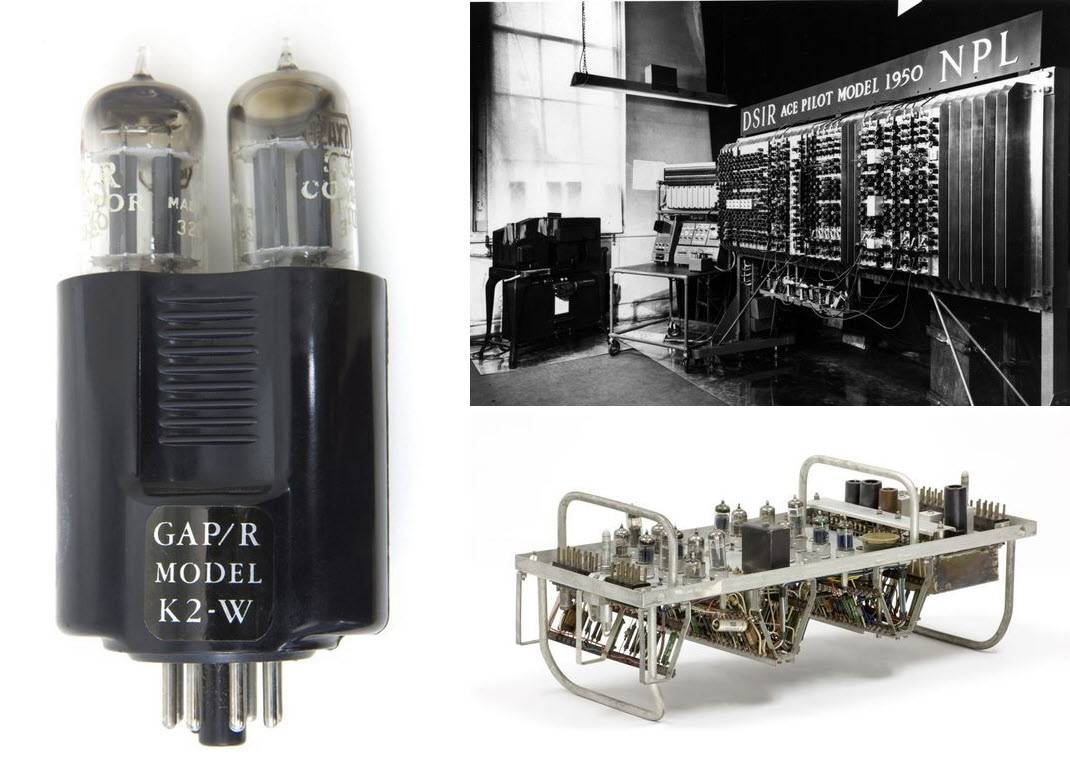
The GAP/R Vacuum Tube K2-W Operational Amplifier, invented by George Philbrick in 1952, has become a classic and has been used in many analog and digital computers. Pilot ACE built by Alan Turing with differential amplifiers in 1950. ALU unit from DEUCE, a production version of the Pilot ACE built in 1955 by the English Electric Company. The 32-bit DEUCE performed 1850 additions per second. (https://www.computerhistory.org)
The differential amplifier works quite simply.
A fixed current flows through the circuit with two arms. If the voltage at the left input is greater than the voltage at the right input, the left transistor turns on and most of the current will go through the left branch, and vice versa.
A small difference between the input signals generates a large change in current, hence the amplifier.
By adding a pair of transistors, we easily get a valve from the amplifier. To do this, you need to fix the voltage in one of the shoulders, calling it the reference. If the input signal is greater than the reference, it is considered "1", and if it is lower - "0". As has been customary since IBM, ground level is usually used as a reference.
As a result, we have a very, very fast circuit that is unstable to interference, consumes a lot of energy and heats up in the same way. Because of the last two reasons, it is difficult to increase the level of integration of ECL chips - a couple of billion CMOS transistors will heat up less and take up less space than 50 ECLs.
The work of Motorola and Fairchild was devoted to overcoming these limitations.
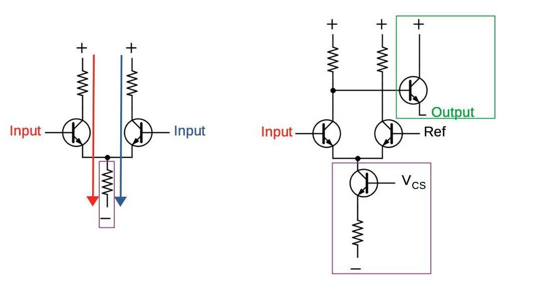
Differential amplifier and inverter based on it. If the input signal is high, the current through the left resistor will pull the voltage down. To increase performance, the lower resistor is replaced by a current sink (purple). The current through the drain is controlled by an external bias voltage. A buffer (green) has been added to the output. The buffer is called an emitter follower, since the output is taken from the emitter of the transistor, and the output repeats the input (circuit from Blog Ken Shirriff).
The first computer assembled on ECL was, as we have already said, the mighty IBM 7030 Stretch, in fact, it was developed for him.
IBM wanted to release a real giant, surpassing the fastest computers at that time by 10–12 times, of course, no already known circuitry was suitable for this.
Stretch's innovation was emitter-coupled logic, created by IBM engineer Hannon S. Yourke. Yurke's switch was a differential amplifier with two 3 volt logic references and required alternating two npn and pnp stages.
This scheme was used not only in the 7030, but also in the scientific 7090, and later - embodied in the form of a GIS in a supercomputer for the NASA System 360 model 91.
By the early 1960s, many emitter-coupled logic circuits had been developed, including variants with Zener diodes, which eliminated the need for 2 types of transistors.
The IBM version for the S/370 (and they did not save money and used ECL literally everywhere in the second line of mainframes), embodied in the form of a microcircuit, was called CSEF (Current-Switch Emitter Follower).
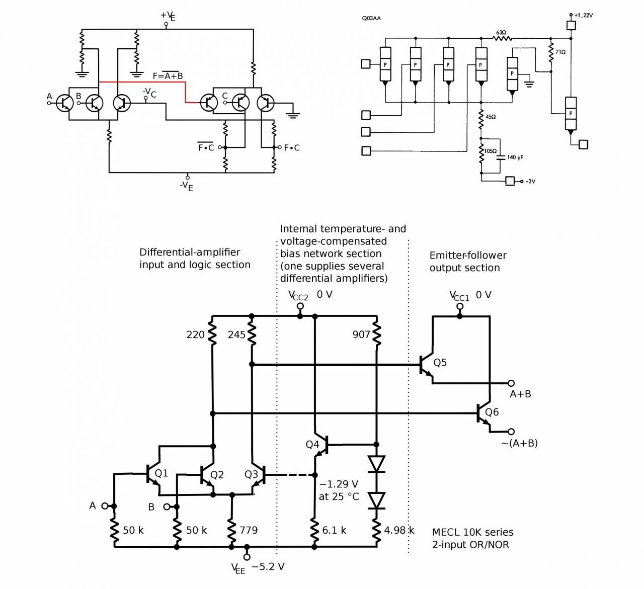
The original Yurke circuit used in the IBM 7030 Stretch, the IBM 360/91 ASLT chip (JL Langdon, EJ Vanderveer, Design of a High-Speed Transistor for the ASLT Current Switch, 1967), and the Motorola 10k base cell.
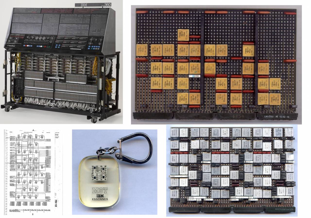
Above: the monstrous console of the IBM System/360 Model 195 supercomputer. With an installation cost of $12,5 million and an additional support cost of $3,3 million a year, it was the most expensive computer of those years. Being a direct competitor to the CDC 7600, made on proprietary ECL microcircuits, the Model 195 surpassed it in power, but was manufactured later and was not popular (only 1971 cars were produced in 1977–20, against 200 from the CDC). One card from Model 195. Notice the chips - they are made by Texas Instruments, this was the only case in storieswhen IBM turned to a third party for help with the release! The cases are also surprising - gilded, metal-ceramic. Each IC contains 2 to 4 gates, usually 3-input NAND. The gate switching time was about XNUMX ns.
Bottom: ALD (Automated Logic Diagram) logic diagram created by IBM EDA (Electronic Design Automation) software for computer-aided design of logic circuits. Branded keychain with MST chip, 4 IC chips are clearly visible. MST card of a 370 IBM System/145 model 1982 mainframe processor. Each chip on it contained up to 5 ECL chips and replaced an entire S/360 board. The Soviet copiers from NITsEVT tried to move along almost the same path in the 1980s, to replace an entire TEZ with one BMK
(http://ibm-1401.info, http://ummr.altervista.org/).
The Soviet response to the IBM 7030 was the BESM-6, which was assembled on a rather sophisticated version of the ECL.
The problem facing the developers was, in general, the same: to increase performance without overly complicating the circuit, but there was one specific feature - the squalor of the domestic element base.
In the mid-60s, Soviet industry was able to produce only two fast semiconductor devices: the D18 diode and the P416 transistor. And those were pretty poor quality. I had to invent cunning circuitry.
The essence is described by one of the designers of BESM-6 V. N. Laut:
The industry produced discrete germanium diodes and triodes with very poor performance.
Was it possible to develop elements for a high-performance machine on them?
... By this time, many reports appeared in the specialized literature about the use of tunnel diodes as the basis for high-speed logic circuits. These diodes had short switching times, many times better than transistors.
However, elements based on tunnel diodes turned out to have poor load capacity, which led to the complication of machine circuits, and we quickly abandoned them ...
The difficulty with using transistors was that they were very slow in saturation mode, and logic elements with unsaturated triodes turned out to be complex due to the need to match the levels of input and output signals.
And not only complex, but also unreliable.
For some time we did not see a way out of the impasse.
A power supply scheme was needed to minimize the number of unreliable transistors, and its key element was invented by the same Sokolov, who later assembled the MCP for Burtsev (and the BESM-6 team split after Lebedev's death, following Melnikov or Burtsev).
The essence of the idea was to introduce an autonomous power source, galvanically not connected to other power circuits, into the well-known "current switch" element.
For example, a miniature battery from an electronic watch could be used for this purpose.
The inclusion of a battery between the collector of the transistor and the collector load (resistor) made the switch an element with consistent levels of input and output signals, and no particularly difficult requirements were imposed on an autonomous power source.
Of course, the battery could not be installed, as it would eventually run out, so in the real circuit it was replaced by a tiny rectifier, consisting of a miniature transformer on a ferrite ring, two semiconductor diodes and a capacitor.
They called these rectifiers "suspended power supplies" (PIP).
The paraphase outputs of the current switches, equipped with emitter followers, could work on the inputs of the logic circuits "AND", "OR".
The following circuitry loomed: passive combinatorial logic based on diode-resistor components was connected to the inputs of amplifying active elements, the outputs of which, in turn, were connected to the inputs of combinatorial circuits, etc.
Thus, the electronic body of the machine looked like a layer cake: layers of diode logic circuits were interspersed with layers of amplifiers on current switches.
Such a structure was very suitable for the implementation of another extremely powerful idea - "assembly work".
To do this, synchronization signals were also brought to the input of amplifiers that act as triggers.
With the light hand of Sergei Alekseevich Lebedev, conveyor circuitry began to be called “water supply” in our country.
BESM-6 was the first Soviet machine to use conveyor work. The pipeline rate, determined by the frequency of synchronization signals, in BESM-6 was equal to 10 MHz.
So, a completely new system of logic elements was developed, which allows squeezing the maximum speed out of the available, not very high-quality domestic transistors and diodes.
Then there was a need to develop the design of such a machine so as not to lose the potential speed of logical elements, as well as technological and easy to use.
In the 50s, there were no multilayer printed circuit boards widely used in modern computer designs.
In BESM-6, printed circuit boards (double-sided) were used only in cells (TEZs), which were of two types: with active trigger elements and passive combinatorial circuits.
The active cells had light indicators on the ends and were installed on the front side of the racks, forming a kind of light panel, passive cells were placed on the back of the racks.
Volumetric backplanes had connectors on both sides, and wired connections passed inside between the connectors along the shortest path.
It was an unusual design. It reduced the size of the machine, and, consequently, the travel times of the signals.
In general, this was probably the most extravagant ECL implementation scheme with an unusual power supply of all possible.
The standard board, the so-called "U" module, from which the processor was assembled (four asynchronous RS-latches), required as many as six power ratings: +40 V, +5 V, -1,6 V, -3,5 V, - 9V, -60V, not counting the variable 6V per suspension power supply (PPS) input, is a total shambles even by early 1960s, let alone 1968 or today.
Technically, the logic in BESM-6 was really implemented on diodes, so in the end it turned out to be something in between DTL and ECL.
A separate bonus was that everything worked in the air - freon was required for the CDC 6600, and it was very difficult and too expensive.
The cooling system of the machine itself weighed more than 7 tons and occupied a separate room (along with food). In BESM-6, they did without such perversions, especially since they did not know how to work sensibly with freon in the USSR even in the late 1980s (we will tell you how much they suffered with the cooling of SSBIS Electronics later).

Block "U" is the basis of BESM, its modern scheme, combinatorial schemes where it was connected, and their implementation in hardware (https://1500py470.livejournal.com)
As you can see, the idea was not bad, while formally the frequency was the same as in the CDC 6600 - 10 MHz (however, this is from the words, what was the real one and the very first versions of BESM-6, purely transistorized, is unknown).
The system architecture - in the form of a horseshoe, which reduces the length of connections and makes it convenient to manage, was also a very good idea, and BESM-6 looked no worse than CDC.
The control, however, was implemented as unbanally as possible - for some sacred reasons, ITMiVT did not like engineering consoles, traditional for machines of the 50-60s (and for large machines - until the 1970s). As a rule, all indication and so on were output to a computer on a separate console.
In BESM-6, in fact, the entire processor was at the same time a console, the lights were displayed on each TEC and briskly blinked during operation!
By the way, it is necessary to explain what it is in general.
The engineering console should not be confused with the terminal; programmers-users of the machine worked behind the terminals. And the console displayed physical information about the current operations of the processor, the contents of all registers, etc. In most cases, it could be changed manually.
Such consoles were made not from a good life, but because old machines required debugging and constant monitoring during the execution of the program.
By the way, in the 1s, many users complained about the lack of such a remote control in the standard configuration of Elbrus-1980.
Traditional engineering console Burroughs B6700 and console processor BESM-6
(http://www.retrocomputingtasmania.com, https://vak.dreamwidth.org/)
(http://www.retrocomputingtasmania.com, https://vak.dreamwidth.org/)
However, the performance of the machine still turned out to be 2,5 times lower, and reliability - 1,5 times less.
What is the reason?
Partly, indeed, the Soviet element base (although compared to the first generation of microcircuits of the 155th series in the EU Row-1, Soviet transistors in BESM-6 can be said to be absolutely reliable).
The main problem was in the system architecture.
The only thing Lebedev had a hand in in this machine was to come up with its command system, and it turned out to be so crooked that, as we will later learn, even the exact implementation of BESM-6 on incredibly fast I200 microcircuits (ECL BMK) did not allow even to increase performance 10 times (although in theory it should have been raised thirty times).
Even the microprocessor implementation of the monstrous Lebedev instruction set from the early 1950s is unlikely to have squeezed more out of BESM-6 than the seedy 386 processor. Still, the element base is far from everything, the architecture of commands plays a big role, which the Lebedev school could never correctly assess.
As for its main competitor, the CDC 6600, Cray also used a rather exotic option in the car - direct-coupled transistor logic (DCTL), something in between TTL and RTL.
DCTL gates have fewer components, are more economical and easier to fabricate on integrated circuits than RTL gates, and are also orders of magnitude faster. Unfortunately, DCTL has a much lower signal level, is more susceptible to noise, and requires matched transistor characteristics because they are heavily overloaded. This is a good feature because it lowers the saturation voltage of the output transistors, but in the case of mismatched elements, it can slow down the circuit.
It works very fast (even faster than ECL!), while it heats up so monstrously that Cray already needed freon in 1966 so that his car would not melt.
In the case of DCTL, the difference between the logical levels is so low (and the switching speed directly depends on this) that with the Soviet element base this circuit would never work at all in principle.
Even by American standards, fine-tuning of selected components was required (the first few pages of the CDC-published book on the 6600 are devoted to how the new silicon transistors made this machine possible), so this model did not become widespread thereafter. Well, because even in the discrete version it heated like an infernal cauldron, in the younger models - CDC 3000 and 1604, the usual DTL was used, although in Cray's version with a couple of subtleties.
DCTL was invented at Bell Labs while working on the first transistor machine in history - TRADIC, completed in 1954. His 1956 version of TRADIC Leprechaun used DCTL.
The main idea of DCTL is as simple as a felt boot - throw out all resistors from RTL.
But how then to switch transistors without driving them too far into saturation?
Elementary: replace the resistors with transistors with special impedances and gains.
This is followed by a long work on the coordination of all this economy. In particular, Cray calculated that the gain of a saturated transistor should be greater than twice the number of output loads, and as applied to the CDC 6600, the rules are: the collector of one transistor can drive five bases within a module, or two local bases within a module and two bases across twisted pair on one other module, and exactly six collectors can be connected within the module.
How cool was the honest 10 MHz squeezed out of such a scheme?
For comparison, the PDP-8, also on discrete transistors, released in 1965 was only 1,5 MHz, and the first IBM PC, released 20 years later, had a clock speed of less than half the speed of the CDC6600, despite being based on the microprocessor. Over the past 20 years, many electronics enthusiasts have revived as a hobby the assembly of transistorized processors.
There are such amateur computers as MT15, Megaprocessor or Monster6502, but, despite all the modern element base and knowledge of new circuit solutions that have emerged over the decades since the creation of the CDC6600, none of the modern transistor computers reaches even 1/10 speed great machine of the 1960s.
Hence, the numbers of 10 MHz on a fundamentally different circuitry in BESM-6 seem doubtful.

On the left is the assembly sequence of the CDC 6600 logical blocks from the Design of a computer the Control Data 6600 book, on the right is the TRADIC DCTL cell diagram and itself (https://en.wikipedia.org)
The logical purity of the CDC 6600 was also ingenious and minimalist.
As with all of his machines, Cray built everything around one single element, in this case an inverter.
Two inverters give AND, two more + AND give NOR, everything else is built on the basis of NOR.
Also interesting is the unusual notation used by Cray and reproduced in the fundamental book Design of a computer the Control Data 6600 written by James E. Thornton, vice president of the CDC Advanced Design Laboratory, in 1970.
Each arrow corresponds to an inverter, circles and squares indicate in which logic the current node should be interpreted - positive (circle) or inverted (square). For both options, the scheme is exactly the same. Each module in the CDC 6600 is built from many basic inverters with one transistor each. This approach was Cray's trademark and recognizable idea - take only one of the simplest things, optimize to perfection and collect everything else on it.
As a result, the CDC 6600 managed to overclock to 5 ns - an absolute record for machines based on discrete transistors, which not every ECL chip can beat. "Elbrus-2" in 1989 had a valve switching speed of only 1,5 times less!
The CDC 7600 was built in a similar way, only with total miniaturization of components - each of its modules consisted of 6 or 8 printed circuit boards connected in cordwood with a freon cooling system, but the CDC 8600 (contrary to the bikes walking on the Internet) should have already been built on ECL microcircuits.
The only problem was that Cray could not get 4 of its parallel processors to work correctly, it took a lot of money and time to fine-tune (in general, parallel programming technology in the 1960s was not developed as much as possible, the massively parallel ILLIAC IV also failed bring to mind), as a result, he became disillusioned with the design of many processors and switched to Cray-1 (and CDC to STAR-100) to vector architecture.
Unique photos. Above - one of the plates of the CDC 7600 module and a comparison of the CDC 6600 and 7600 modules. Below - the module in the assembly and a view of 6 and 8 plate modules
(https://cds.cern.ch, https://vaxbarn.com, https://people.cs.clemson.edu)
(https://cds.cern.ch, https://vaxbarn.com, https://people.cs.clemson.edu)
Motorola became the icon of ECL.
In 1962, they developed an original topology, modestly and simply called Motorola ECL (MECL).
The first microcircuits using this technology, MC30x/MC35x, were produced in characteristic tablet cases and had good parameters: 8–8,5 ns delay, frequency up to 30 MHz – remember that microwave transistors (well, at that time, microwave) CDC 6600 , released 2 years later, gave out 10 MHz.
The second generation was called no wonder - MECL II (1966), and it corresponded to the MC1000 / MC1200 microcircuits with a delay of 4 ns per gate.
Finally, in 1968, the third generation of logic was developed, which became so successful that it lasted on the assembly line until the mid-1980s.
MECL III corresponded to the MC16xx series chips, which, depending on the year and type, operated at frequencies from 150 MHz (MC1658 Voltage Controlled Multivibrator) to 1,2 GHz (MC1699 Divide-by-Four GHz Counter).
In variants of the 1980s, MECL III allowed the design of chips with up to 10 gates, overclocked to 000–0,1 ns.
From stocks of ebay - Motorola MC350, MC1000, MC10000 and quite a rarity - an unopened package of silicon wafers for the production of their chips
(https://www.ebay.com)
(https://www.ebay.com)
In 1971, Motorola decided to make a small branch of its line and make chips intermediate between the already slightly slow MC1000 and the space-fast MC1600, although by this time the speed of the MC1000 had doubled (for example, MC1027 / MC1227 120 MHz and MC1034 / MC1234 180 MHz , with a delay time of 2 ns, instead of 4 ns for the first copies of 1966).
Thus the MC10000 series was born.
It differed from MECL III only in resistor values, the circuitry was completely the same.
The first versions of the MC10k had delays of up to 2-3 ns and a frequency of up to 125 MHz, and most importantly, reduced power consumption and heat dissipation compared to MECL II / III. As always, 2 series were released - the military MC10500 (and MC10600 earlier) and the civilian MC10100 (and MC10200 later).
In the lineup, there was a place for such a then-popular thing as BSP - its role was played by a 4-bit MC10800.
This line was followed by the MC12k (1976) at 250 MHz and the MECL 10H (1981), and in 1987 came the ECLinPS (Picosecond ECL, 0,5 ns) at 1,1 GHz.
However, Motorola did not become the greatest manufacturer of American ECL logic.
In 1973, Fairchild announced the F95K, F10K and F100K.
These lines are amazing in combination of two things - how little they know about them (even on the English-speaking Internet there is practically nothing, everything needs to be dug out from books and manuals) and how great cars were assembled on them.
The F10K was a further development of the MC10000 and differed significantly from it.
Due to the difficult fate of Fairchild in the 1970s (all the top developers and managers left it, having founded all sorts of Signetics, Intel and AMD, and it was somehow necessary to produce chips), the production of the F10K hung up for a couple of years until 1975.
It was the world's first fully voltage and temperature compensated ECL circuitry, as a result, the crystal was heated much more evenly, and this greatly reduced noise and temperature instability.
The F100K was an ultra-fast version of the F10K, accelerating to 0,7 ns.
All lines were assembled using proprietary Isoplanar II technology, civilian cases were small DIP24. The F100K itself was a series of small loose pieces, its subtypes were the larger F200 (basic matrix crystals for custom microcircuits) and the powerful 8bit BSP F220 (appeared in 1980, marking 10022x).
And a similar selection for the Fairchild F100, including developer's books
(https://www.ebay.com)
(https://www.ebay.com)
It was already possible to assemble something really serious on such chips, and it did not take long to appear - a year after the release of the series, Seymour Cray assembled his great Cray-1 on it.
The entire machine of the first version was implemented on only 4 types of microcircuits: Fairchild 11C01 (dual OR/NOT), Fairchild 10145A (64-Bit RAM), Fairchild 10415 (1024-Bit RAM) and Motorola MC10009 (a cheaper analogue of 11C01 in address fetch schemes). ).
Interestingly, the logic was implemented, in fact, on one type of elements - 2OR-NOT.
It took 250 such microcircuits, and 000 memory microcircuits.
Naturally, not only Cray took advantage of the joy, DEC released the PDP-10 on the SN74LS in 1974, and a year later transferred older models to the F10K.
In 1977, improved 4Kbit RAM chips appeared, and the Cray-1 experienced a memory upgrade.
In the same years, Motorola licensed the F100K back to itself and suffered for a long time, trying to create an analogue, rolling it out only in 1981 as the MC100k (an improved clone of the F200, called MCA - Macrocell Array), but immediately came out with a wider range and overshadowed the original (in as a result, Cray-2 and CDC CYBER were already assembled on it).
Throughout the 1980s, on the F100K architecture, they produced a bunch of all kinds of specialized and simply powerful machines, including such exotics as, for example, the 64-bit real coprocessor Floating Point Systems FPS-264 (1985), which accelerated 5 times compared to the FPS-164 on SN74LS.
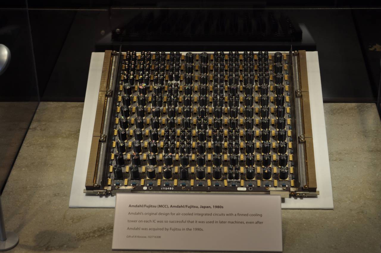
IBM began production of its ECL chips for the S/370 in the late 1960s, and the Japanese were no less distinguished: Fujitsu developed original ECLs for itself and Amdahl (and copied under the F100K license), in Europe ECL was manufactured by Siemens.
A bunch of processor boards from Cray-1 and the principle of mounting them in a cooling rack
(https://www.digibarn.com/ and https://www.computerhistory.org)
(https://www.digibarn.com/ and https://www.computerhistory.org)
The main commercial ECL-BMC series of the second half of the 1980s was the Motorola MCA3 ETL.
These were powerful chips made according to the proprietary MOSAIC III process technology with a mixed interface that supports ECL, PECL (a more advanced version of Positive ECL emitter-coupled logic with +5 V supply) and TTL chips. The delay was no more than 150 ps, full-fledged QFP, PGA and TAB packages were used, and there were from 858 to 6915 gates. The chips were simply marked, according to the number of gates available: from MCA600ETL to MCA6500ETL.

Motorola MCA 3 construction from datasheet
ECL's superior power consumption and heat dissipation meant they could only be used in top-tier liquid, immersion or cryo-cooled systems.
In principle, rather slow chips could live with air, but for the most part they usually installed something more powerful.
IBM ES / 3900 (by the way, they thumped for about 10 years and as many billions to develop the multi-chip TCM module - Thermal Conduction Module, for them, in fact, it was then that multi-chip processors, so popular in our time, were invented), Amdahl 470 / V6, all the Japanese supercomputers of the 1980s, of course, the Cray-1 and Cray-2, the older DEC models from the KL10 PDP-10 to the VAX 9000, all used ECL.
The famous Tandem series of fault-tolerant machines, which we already wrote about, used SN1983AS in its TXP server (74), but already took ECL for its flagship NonStop VLX (1986).
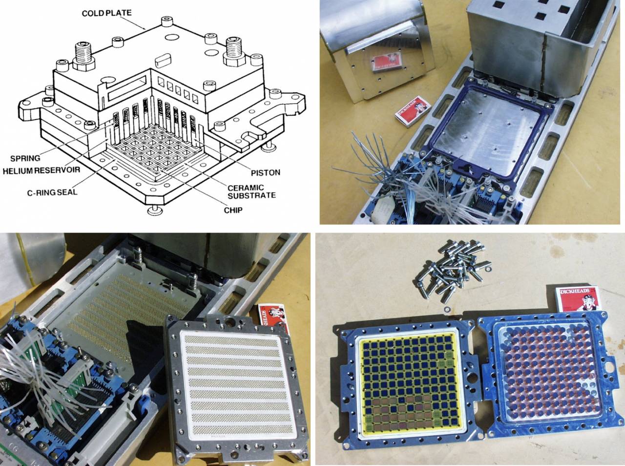
Incredible TCM is a technology that IBM has spent about 10 years and more than a billion dollars
(https://www.researchgate.net, http://members.optusnet.com.au)
(https://www.researchgate.net, http://members.optusnet.com.au)
An even more incredible Amdahl 470 mainframe processor and Fujitsu mainframe board from it, all made on BMK's ECL. A completely similar scheme was used by the Fujitsu FACOM M-190 mainframe. The car itself is in the background. Such boards now cost 2-3 thousand dollars among collectors.
(https://i.redd.it, https://www.flickr.com/)
(https://i.redd.it, https://www.flickr.com/)
Another S/370 clone is the 1982 National Advanced System AS/XL mainframe processor. 8 eight-bit BSPs (National Semiconductor's F220 clone) form a 64-bit processor. In total, about 30 custom microcircuits were developed for the mainframe on MECL 10K and MECL 10000 MCA.
In 1984, DEC tried to release the "IBM killer" - the most powerful VAX 9000 mainframe.
The company planned to invest about a billion dollars in development, despite considerable employee concern that RISC processors were rapidly catching up with multi-chip systems at BMC.
However, by that time, the PDP-11 could still fit in a single-chip version (J-11 processor), the classic VAX no longer existed (only its MicroVAX 78032 version).
In 1980, Gene Amdahl created Trilogy Systems to improve ECL technology for his mainframes, and DEC licensed his designs.
In the final version, the VAX 9000 processor was implemented as an IBM-type multi-chip module, out of 13 BMCs of the original architecture ordered from Motorola. During development, in 1988, IBM rolled out the AS/400 server (which generated more than $14 billion in sales—they alone made more money than all of DEC), hitting the VAX segment.
At the same time, Sun introduced its SPARC microprocessor, which enabled desktop machines to outperform even the fastest existing DEC machines.
I just don't understand it, I don't see how this is possible, how this one chip can replace these racks of electronics, I just don't get it!
exclaimed the unfortunate DEC director Ken Olsen, stuck like the Soviet academics in the 1960s.
Engineers tried to persuade him to cancel 9000, explaining that by the time it was released it would not be the most powerful mainframe in the world, but just an ordinary server, only 1 times more expensive, but Olsen stood his ground, like our ministers and developers.
In the end, DEC pumped over $3,5 billion into the project and only completed it by 1990, offering a machine comparable to the IBM 3090 for about $4 million. Only 40 9000 systems were produced and sold - by then it was obvious that CMOS microprocessors had ascended the throne forever.
In 1991, NVAX appeared - a system for a healthy person, developed by a group of adequate DEC engineers, with the performance of a VAX 9000, but in the format of a conventional microprocessor.
It allowed the company not to die, but became the last in the glorious VAX line - on the way was the DECchip 21064, better known as Alpha, the most powerful and best processor until the early 2000s.
VAX 9000 became, in a sense, an analogue of "Electronics SSBIS" - developed on pure perseverance and stupidity, expensive and useless.
The only difference was that the hands of DEC engineers grew from the right places (and not like in the Delta Research Institute), as a result, the car had air, not freon cooling, was 20 times smaller, just as fast, development took 5 years , not 10, and she still reached serial production.
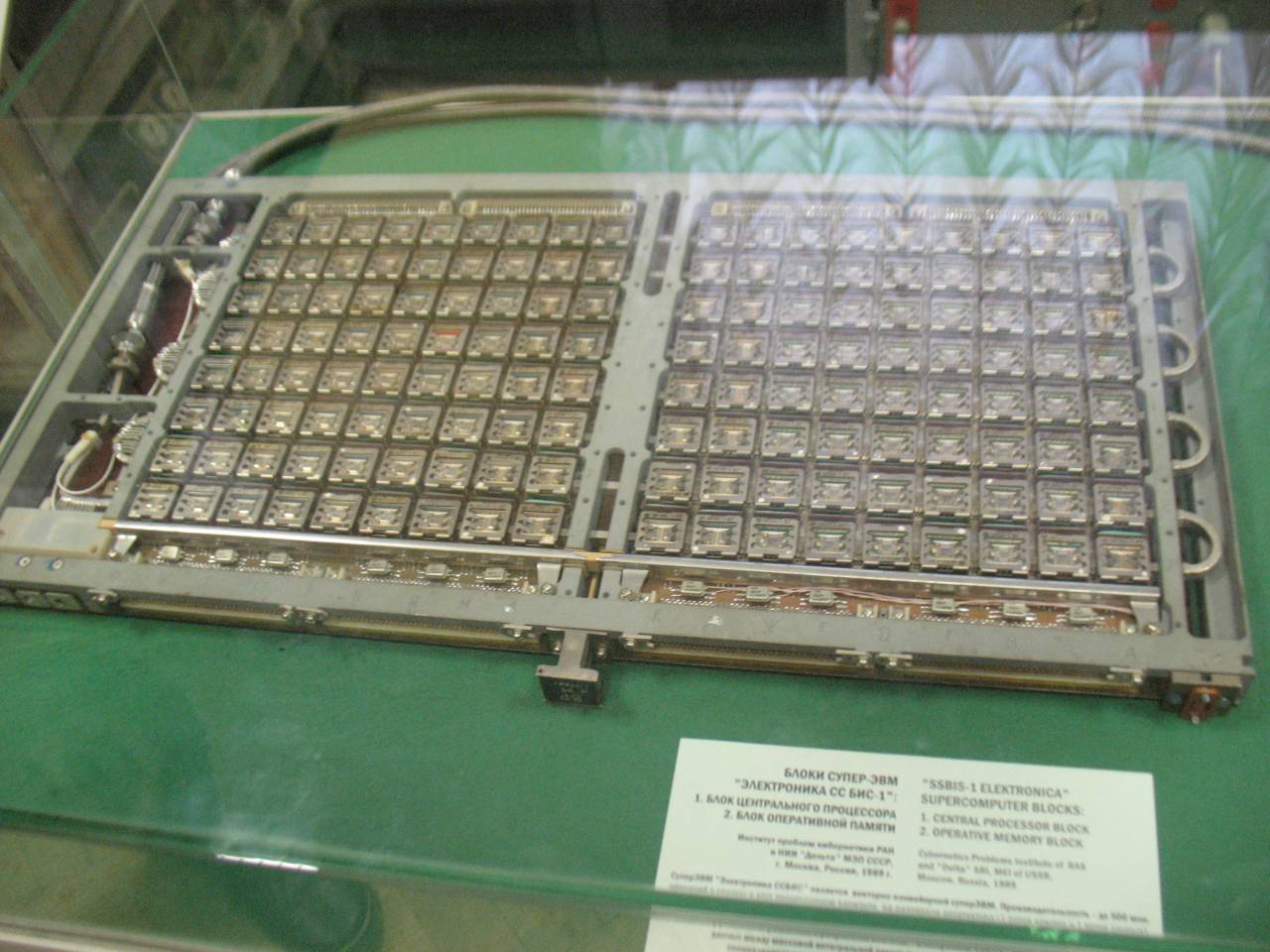
For comparison: SSBIS Electronics, a prototype partially launched in the same year, was a set of cabinets from an assembly hall containing 5 kilos of gold, hundreds of kilometers of hand-wired coax, a processor on multilayer sandwiches of freon-cooled discrete boards on hundreds of ECL chips , which could not be overclocked even to the passport 75 MHz, got stuck at 66.
And yes, in terms of performance, all this was approximately equal to the VAX 9000, and the development took 10 years, an unimaginable number of millions and the efforts of the entire Delta Research Institute, crowds of elderly academicians and heaps of enterprises.
After such a domestic microelectronics, I want to shoot out of pity, which, in general, happened in 1991.
Absolutely marvelous VAX 9000 processor on a heap of BMK. Strictly speaking, this is not a complete processor in the modern sense of the word, the machine was assembled from various modules made in such a construct, among which were DISTRIBURITON UNIT, INTEGER UNIT, MULTIPLICATION UNIT, FLOATING UNIT, CONTROL UNIT, VIRTUAL INSTRUCTION CACHE, CROSSBAR UNIT, MICRO CONTRO STORAGE and others. The first photo shows P1004 FAD (EBOX FLOATING UNIT), the purpose of the following technoarchaeologists has not yet been clarified
(photo from the collection of user pixelmanca, https://www.cpu-world.com/forum/)
(photo from the collection of user pixelmanca, https://www.cpu-world.com/forum/)
And for comparison, a car inferior to it in all respects, but of the same year - "Electronics SSBIS".
Photo from the collection of the Polytechnic Museum in Moscow (https://1500py470.livejournal.com)
Photo from the collection of the Polytechnic Museum in Moscow (https://1500py470.livejournal.com)
ECL in processors is dead forever, but its last and most exotic use was in microprocessors!
The firm Bipolar Integrated Technology, the largest expert on bipolar technology in the early 1990s, decided to squeeze everything possible and impossible out of it. They collaborated with two RISC pioneers, MIPS Computer Systems and Sun Microsystems, to create an ECL processor of unprecedented power based on RISC architectures.
The first implementation of the MIPS II architecture, a set of R6000, R6010 and R6020 chips, was made as an MCM module and was used in high-performance Control Data Systems 4680-300 Series InforServer servers (they were tried to be produced by the former Control Data Corporation, reorganized in 1992).
By the way, they overclocked it to 80 MHz, and it doesn't look close to the records available by ECL, but the processor did not burn the board through. A SPARC B5000 was made for Sun, about which there is almost no information.
Finally, the craziest chip on the ECL was an experimental microprocessor from DEC, who managed to shove MIPS II into one chip!
For 1993, the most powerful general-purpose microprocessor was the Intel Pentium at 66 MHz with a TPD of 15 watts. DEC MIPS II had 300 MHz (!) and 115 W (!) - heat dissipation at the level of Core i9. A separate article was devoted to the cooling of this monster.
CMOS, however, conquered such frequencies after 2-3 years with heat dissipation 3 times less, and the insane ECL was forgotten.
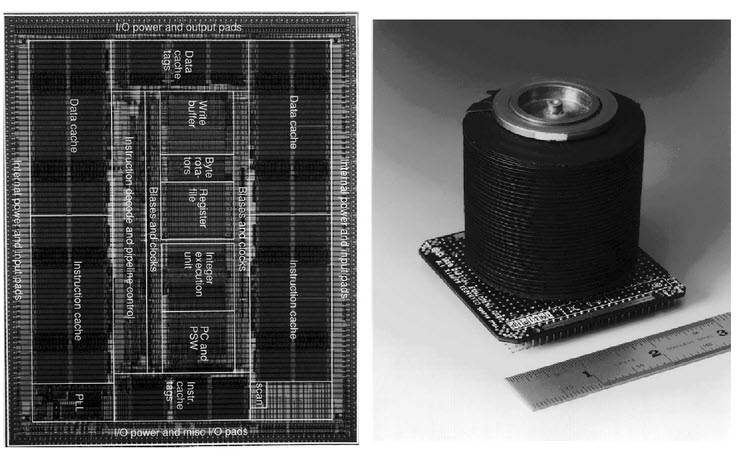
The same DEC MIPS II monster from the 1993 article A 300 MHz 115 W 32 b bipolar ECL microprocessor with on-chip caches in the IEEE International Solid-State Circuits Conference Digest of Technical Papers. Photo R6000 and B5000, alas, could not be found.
BMK and how to cook it
Before moving on to the Elbrus-2 element base, let's talk about how they worked with the BMK in general in the West and what kind of beast it is.
The 1970s was the era of low-to-medium integration chip assembly, which meant that it was one or more boards studded with chip rectangles (we're talking about serious machine processors, of course, not microprocessors).
In 99% of cases, the hardware companies themselves were involved in the development and manufacture of the processor at all levels.
With the early 1980s came the era of LSI and two new ways to make your own architecture.
Firstly, it was possible to assemble it on a BSP for every taste, speed and budget: from the tiny and slow TTL Intel 300x to the powerful 8-bit ECL Fairchild F220.
In this case, the manufacture of the processor was reduced, in fact, to the development of a system of commands and its firmware in the attached control device.
The second method came in handy when the architecture was too powerful or too conceptual to be implemented in a standard way.
Chip makers quickly realized that if you only offer ready-made standard solutions, you can miss customers who want something special at an additional price.
This is how the concept of custom-made chips was born based on what in the USSR they called BMC, basic matrix crystals, and in the West - Gate Array.
FMC is a semi-finished chip for ~15-50 gates, its only difference is that most transistors do not have a predefined function. They can be connected with metallization layers, forming standard NAND or NOR cells, and then assembled from them into a complete circuit with the next layer.
Thus, pure BMC exists only in the advertising brochure or in internal warehouses - all chips that finally leave the factory already have a strictly defined structure.
BMK master wafers with unfinished chips are usually manufactured in advance and stored, as a result, the design of the processor is reduced to throwing its topology into the CAD system, and then the wafers will go further to the conveyor, where this topology will be reproduced in them, cut, packaged and delivered to the client.
Perhaps someone has heard of something similar, and yes, now a similar technology is called application-specific integrated circuit (ASIC).
ASIC is already a full-fledged SoC, including, as a rule, I / O, controllers and memory, they are used in a huge number of applications, they run a bunch of various embedded equipment, and also, for example, Bitcoin miners.
The main difference is that ASICs are designed from already formed standard cells, and not bare transistors, like BMCs.
Of course, BMKs were supplied by whole families, differing in the number of valves and in price.
As a result, each computer manufacturer could choose a chipset that optimally fits its instruction set.
Of course, there are subtleties, for example, a cross matrix switcher requires much more connections and, accordingly, layers than a similar systolic array, while the complexity of the circuit purely in terms of the number of valves will be approximately equal.
Unused lanes and gates increase the complexity and cost of the chip, both for the manufacturer and the customer, so it is a great art to design the BMC in an optimal way to suit most applications.
As a result, their creators tried to provide the number of tracks that would be enough to route most of the topology potentially possible on so many gates.
This is often helped by Rent's empirical law, discovered by one of the IBM engineers in 1960 (Rent, EF: Microminiature packaging. Logic block to pin ratio. IBM Memoranda, November 28 - December 12 1960). It states that the number of microcircuit pins is equal to the average number of interconnects per logical element, multiplied by the number of logical elements to the power of R, where R is the Rent constant (for example, for microprocessors R \u0,5d 0,74 - XNUMX).
Bipolar arrays were invented by IBM in 1966 (IBM Journal of Research and Development Volume: 10, Issue: 5, Sep. 1966). It was then that they described the technology of what in the future was called semi-custom schemes, and IBM called the master slice technology.
Already during the design of the S/360, it became obvious that the next machine would have to use ICs.
IBM has never bought anything from anyone in principle, making everything for its computers on its own, right down to the last bolt.
Naturally, they developed their own line of microcircuits, which never entered the open market, and an absolutely original technology for their manufacture, up to characteristic cases - not dull DIPs, but recognizable metal cubes.
Since they needed a huge number of chips, their engineers found a way to drastically reduce production costs. They developed a series of several general-purpose silicon dies, which were then metallized with tracks, connecting them in the required order. Such a disc was called master slice. Even then, IBM used computers for design.
Fairchild jumped at the idea and released the world's first commercial series of custom Micromatrix chips (a 32-gate DTL array with 20 ns latency) a year later. In 1968, two variants of Polycell TTL matrices (up to 144 gates, 18 ns) were released.
At the same time, three more companies announced such toys: Sylvania SL80 (30 gates), Motorola (25 and 80 gates, 5 ns) and TI Master Slice (several cells of 16 gates).
Raytheon joined in the festivities in 1971, and in 1973 they released the TTL(S) RA-116, which was in production until the 80s.
Around this time, major manufacturers such as RCA and Hughes also entered the BMC business.
In 1972, the British Ferranti rolled out the first version of its ULA (Uncommited Logic Array), and later even bought the American BMK manufacturer Interdesign. By 1983, they had reached 10000 gates on the circuit.
CMOS opened up the widest possibilities for the production of custom chips, the first CMOS-BMCs were created by Robert Lipp in 1974 for International Microcircuits, Inc. (IMI).
CAD technologies in those years were very primitive, so most of the design work was done by hand. In 1978, Lipp founded IMI competitor California Devices, Inc. (CDI).
Since 1976, the heyday of the BMC has come.
Fairchild and Motorola returned to the market with their ECL and Texas Instruments with I2L and STL.
In Europe, at least four manufacturers (Ferranti, Philips, Plessey and Siemens) were involved in BMC, and in Japan Fujitsu, Hitachi and NEC were the most notable.
Fuseable jumper programmable FPLAs appeared at Signetics in 1975 as a result of developing the technology for manufacturing nichrome jumpers used in ROM.
In the same period, microprocessors appeared and disputes broke out about which development option would win.
A variety of custom chips and FPGAs for every taste and budget, 1985–1995.
(https://www.ebay.com)
(https://www.ebay.com)
For ten years, BMCs were considered serious competitors to microprocessors (probably, 70 percent of large and medium-sized machines were assembled on them), and it was not even predetermined which approach would win.
In 1979, VLSI Technology was founded, as usual, by Fairchild alumni Jack Balletto, Daniel Floyd, and Gunnar Wetlesen, in company with Doug Fairbairn of the Xerox PARC project.
From the very beginning, the company focused on the development of chips on order, relying on the intellectual resources of nearby Caltech and the University of Berkeley. VLSI became the first supplier of ASICs - custom microcircuits based on standard cells in the early 1980s, and the second company, LSI Logic, was a leader in the production of microcircuits based on classical BMCs.
LSI Logic was established in 1981 in the same sunny California and by 1985 had built a huge plate manufacturing plant in Tsukuba (Japan) together with Kawasaki Steel.
In 1983, by order of the US Department of Defense, the VHDL (VHSIC Hardware Description Language) specification was developed, designed to formally describe logic circuits for all stages of development.
In the same year, Automated Integrated Design Systems was founded, created to develop CAD circuits, and their first product was developed - an analogue of VHDL, the Verilog language.
IBM contributed to the rise in popularity of custom solutions when, in 1981, it introduced its most powerful next-generation mainframe, the IBM 3081, with a processor completely assembled from BMC ECL.
In the UK that same year, at the opposite end of the performance spectrum, Sinclair builds the ZX81 (the forerunner of the home PC icon, the ZX Spectrum) on the Ferranti ULA BMK (cloned in the USSR as the T34VG1).
Heavy metal in Japanese. These are all basic matrix crystals. Fujitsu FACOM M-780 of 1987, the most powerful IBM-compatible mainframe in the world at that time and the first mainframe with a processor on a single board. This is what Row-4 of a healthy and rich person would look like. On the left - a block of main memory from modules made entirely according to modern technology, and an unimaginable processor - on the right: a 54x49 cm board (!) With 336 BMCs (!), Placed as a sandwich between two cooling plates with individual copper heat sinks to each crystal. Next: NEC and Hitachi also had monster boards, the Hitachi HITAC M-68X processor (1986) and the NEC ACOS System 1000 (1980)
(http://museum.ipsj.or.jp)
(http://museum.ipsj.or.jp)
Further, the market was unstoppable.
In 1983, Altera was born, offering a fundamental novelty to the market - the reconfigurable user-programmable chip EP300.
In 1985, Ross Freeman and Bernard Vonderschmitt invent and patent a new way to create such arrays, called a field-programmable gate array (FPGA).
With the release in the same year of the first FPGA XC2064, the history of Altera's main competitor, Xilinx, begins.
Its first products were in many ways similar to the early BMCs - slow and expensive, suitable only for some niche markets. However, Moore's Law quickly made them a force, and by the early 1990s they had seriously disrupted the market for custom chips.
Finally, Cadence Design Systems was founded in 1988, a company that took automated chip design to the next level and now offers design systems licensed for millions of dollars.
Almost all modern microprocessors from Intel Core i9 to Apple M1 are created in Cadence CAD. Classic BMCs died out by the mid-1990s, supplanted by FPGAs, ASICs and microprocessors, but their influence on the development of computers was colossal.
So, how did the development of a custom ECL chip on the Fairchild F200 BMK look like in 1981?
Let's turn to the advertising brochure of the company itself.
Using the fastest ECL family for its F200 BMK, Fairchild maintains compatibility with the F100K.
Development is carried out almost entirely on the computer.
Fairchild charges an entry fee of $20 to $000 and provides training (25 to 000 weeks) on the use of our Cybernet computer network.
The creation of the BMC using macrofunctional cells is done manually, but the next steps (generation of test vectors and verification of the design) use the TEGAS program on Cybernet.
Linking and placement of macros is partly done manually, partly with the help of a computer; the design rules are checked by the computer.
Computer time charges range from $5 to $000, depending on your level of experience.
Making a basic mask for an F200 array costs between $10 and $000; Fairchild will also do the design and packaging for an additional $15-$000 (now you know why mainframes are expensive).
Fairchild F300 FGA2000 - a powerful BMK of the 1980s, the dream of Soviet developers
(https://1500py470.livejournal.com)
(https://1500py470.livejournal.com)
As you can see, the use of BMC technology requires a significant investment of time and resources; you must work with the chip manufacturer to create system logic diagrams, functional test sequences, convert logic to gate array patterns, software and hardware simulations, interconnect diagrams, mask development, and prototyping.
In the USSR, all this fell on the shoulders of individual institutes, of which there were three, and they were competitors: ITMiVT (Elbrus-2 of the second generation), NITSEVT (ES Computer Ryad-4) and Research Institute Delta (Electronics SSBIS).
ITMiVT and NITSEVT belonged to the MRP, and Delta belonged to the MEP, and MEP owned 90% of the microchip factories.
As long as Shokin's friend Kalmykov was alive, this was no problem for the MCI. With the change of minister to Pleshakov in 1974, the process of cooperation slowed down.
In addition, the situation was aggravated by intrigues between three groups of developers - Przhiyalkovsky with ES computers and Burtsev with Elbrus-2 inside the MRP, and Melnikov with Elektronika SSBIS from the MEP.
The MEP also wanted its own supercomputer, and by expelling Melnikov into it in 1974, Burtsev created a dangerous competitor for himself.
In the early 1980s, the SSBIS Electronics project was adopted, for which BMKs were also needed, and in the most critical period for Elbrus-2, cooperation between MCI and MEP hung in the balance.
I had to bow to internal competitors - NICEVT in their famous headquarters, a 700-meter "lying skyscraper" on Varshavsky, the longest scientific building in the world. In this skyscraper, in the adjacent rooms, employees of the NICEVT and ITMiVT jointly tinkered with the theme of BMC.
It is not surprising that the development of the BMK took several years in the Union.
Even in the USA, in the homeland of technology, where it was thoroughly studied from the very beginning and where the microelectronic business worked in those years simply at the limit of human efficiency (taking into account what crazy, unimaginable money was spinning there), the full design cycle of the BMK took in 1980- e years from 6 to 12 months.
At that time, only the Japanese surpassed the Americans, who were already working at the limit of not human, but the efficiency of biorobots, so 4 giants - Fujitsu, NEC, Toshiba and Hitachi (and Amdahl, who wisely ordered BMC from the Japanese from Fujitsu) tore the American market to shreds, until Reagan didn't intervene with protective measures (and until IBM dirtyly sued Gene Amdal for daring to release a machine compatible with the S/370 but twice as good).
If we take into account that each scheme required, as a rule, several iterations to perfect the architecture, and the cost of a negligible mistake was a batch of thousands of chips, it is not surprising that only very, very thick companies could afford to work with BMK for very solid projects.
As a result, the delay between the announcement of the new BMK technology and real machines on them was 3–4 years, even in the case of the United States - in fact, with all the quality of Soviet microcircuits, it’s just a miracle and a feat that they were mastered to release in 6–7 years.
The monstrously wealthy Fujitsu, with a staff of thousands of engineers and a full production cycle, could afford to release a mainframe for Amdahl in 1980 on a BMK with 10K valves, and the development of the Cray X-MP supercomputer by the efforts of several people on tiny compared to Fujitsu with only 16 valves matrices was completed only in 1982.
The CDC wrote in the ad:
CDC uses the fastest Fairchild F200 family of ECLs of its time, compatible with the Fairchild F100K series, so that these BMCs and standard circuits can be combined to reduce the number of required options.
Designing with the F200 is very costly.
Development is almost entirely done on a rental computer at Fairchild via customer terminals.
Designing with the F200 is very costly.
Development is almost entirely done on a rental computer at Fairchild via customer terminals.
A reasonable question arises.
CDC and Cray were literally at the peak of technological progress in the 1980s and 1990s, being tiny in the state, they managed to survive in a society crowding around the giants Fujitsu, IBM and UNISYS. At the same time, they produced computers manually, and the number of each model was estimated at only tens of pieces.
Their business was always going on, limping on both legs, how did they even survive?
And where did they get crazy money for development over and over again, always going to zero in terms of profit?
And why, with all the talent of their engineers, this scheme suddenly stopped working in 1990?
The answer to this question has a name.
Ronald Wilson Reagan.
As we have already mentioned, the 1970s were the golden age of the Soviet partocrats.
Continued detente, petrodollars, technical cooperation with the United States. For the first time since the late 1950s, our people were again allowed to use Motorola, it got to the point that in 1975–1976 negotiations with IBM on normal licensing of the EU were quite productive (taking into account that the whole world was already so busy with this - and the Germans , and the British, and the Japanese), and at Motorola we legally bought packs of MC10k.
However, the process dragged on for a couple of years, and then unforeseen events happened that put an end to all plans. Afghanistan, the uprising of "Solidarity" in Poland and the martial law in it and, like a cherry on the cake - the death of Brezhnev and the coming to power of "mini-Stalin" - Andropov.
Reagan, of course, used all this as a casus belli, and the final powerful round of the Cold War followed, which finished off the USSR in 10 years.
The U.S. government invested the most in a decade since World War II in a variety of dual-use R&D, which led to an incredible riot in the 1980s of the strangest, exotic, and unique architectures and machines.
And since 1990, the need for an infusion of funds has disappeared, and the market has remained to decide the fate of everything that was invented in the fat decade.
As we know, he decided: over the next 5 years, RISC microprocessors and their massively parallel architecture won the competition, displacing the whole marvelous zoo.
CDC received direct investment from the government with the departure of Cray in 1972, and this allowed it to still complete the completely unprofitable STAR-100, which had enormous difficulties in designing (given that one connection with the PDP-11 control computer there was implemented on as many as 4 types of ECL BMK, 168 valves each).
In fact, the whole STAR project was a front for the development of three systems: Flexible Processor (FP), Image Processor (IP) and Advanced Flexible Processor (AFP), also known as Cyberplus, designed to process photographic images and radar data for the CIA and the NSA.
By 1986, at least 21 Cyberplus multiprocessor installations on custom chips had been installed. These parallel processing systems included from 1 to 256 Cyberplus processors providing 250 MFLOPS each, which are connected to the CYBER machines via direct memory attach architecture (MIA).
The number of FPs and IPs released and installed is unknown, the last CDC military product being the Parallel Modular Signal Processor (PMSP) released in 1988.
So the development of the BMC on the ECL was generously paid for by the American government.
In general, an incredible number of secret architectures were released in the USA, mainly for the NSA and the CIA, many cryptocomputers are still classified.
For example, the National Cryptologic Museum demonstrates a certain MC100k board called CLAW 1 and says that it was installed already in the CDC 7600 (!), but, most importantly, no one knows why, and there is no information about it.
Advanced Flexible Processor architecture and the mysterious CLAW 1 board on real ECL from Motorola
(https://1500py470.livejournal.com, https://en.wikipedia.org)
(https://1500py470.livejournal.com, https://en.wikipedia.org)
At this time in the USSR
In the USSR, the history of ECL began, who would doubt it, with the same Motorola.
We sometimes mention that the transition to copying the BMK series 10k, as usual, ruined the unique Soviet developments, presented in the late 1960s by series 137, 187, 229 and 138.
Our beloved Malashevich recalls:
An interesting example is the creation of the ESL IC series 100.
As far back as 1969, NIIME had developed its own technology for the production of ESL ICs and delivered the first samples of several original ICs of the 138 series.
But soon the development of the Elbrus supercomputer began, and at the request of its chief designer (supported by a resolution of the Central Committee of the CPSU and the Council of Ministers of the USSR, which you can’t argue with), NIIME and Micron were entrusted with the reproduction of the Motorola MC10000 series.
It was neither expedient nor feasible to produce two series of ICs with similar characteristics, and beyond the power of NIIME and Mikron.
As a result, the development of the original K138 series had to be stopped and, to please the customer, analogues of the long-produced MC10000 (series 100) were made, inferior to the K138 series in terms of speed (the most important parameter for ESL ICs).
In fact, here, as usual, everything is so and not so.
Actually, immediately with the founding of Zelenograd in it (as new factories were launched and new research institutes were built), more and more new copy lines were deployed in it. Together with TTL and DTL, the chipping of ECL chips began in the mid-1960s.
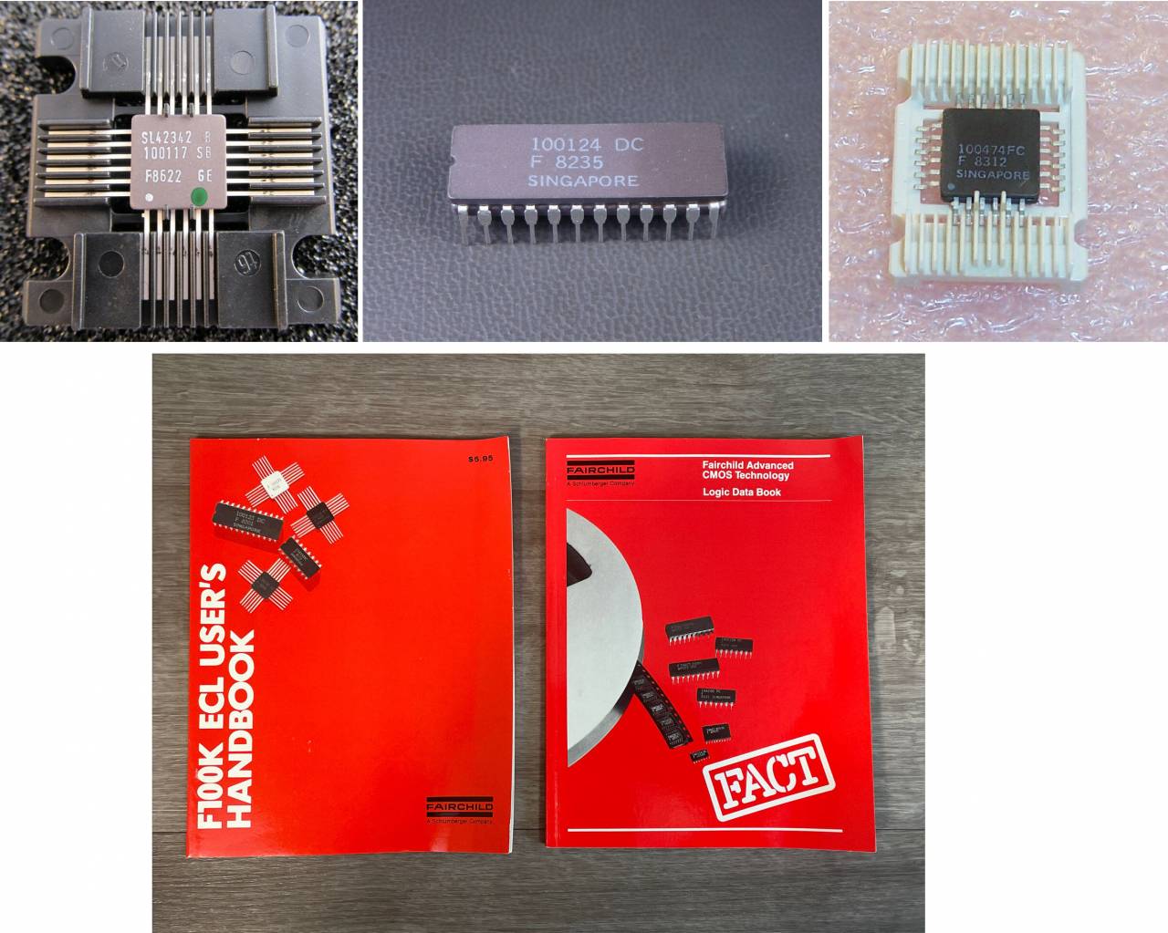
The very first Soviet ECLs are the rare D34 and D35 series, a prototype that appeared in 1968 and is an exact clone of the Motorola MECL-I. A year later, their slightly improved version came out - the 137th series (in a planar gold case for the military, known as 191).
Initially, they were developed by order of Przyjalkowski from NICEVT to assemble the flagship of the first row of the EU - the EU-1050. It had a three-stage asynchronous pipeline and a performance of 500 MIPS, in principle, not bad.
The EU-1060 was supposed to be the flagship in general, but they didn’t have time to make it and transferred it to Ryad-2.
The team for the development of the R-500 machine, which later became known as the EU-1050, was formed in 1968 (they originally wanted to make 4 options: R-20, R-100, R-500 and R-2000), in the same year development of the 137th series began.
Yuri Lomov, a participant in the development of the EU-1050, recalls:
... The element base (integrated logic circuits of medium integration ECL137, ECL138 and ferrite cores as memory elements), although significantly inferior to foreign ones, still made it possible to implement the proposed computer architecture.
So, we did not expect any difficulties in meeting the performance requirements (500 op/s) from the point of view of the architecture's capabilities.
So, we did not expect any difficulties in meeting the performance requirements (500 op/s) from the point of view of the architecture's capabilities.
As a result, the 137th series was a 1962 MECL I clone, and the 138th (with a delay time of 3 ns) was a MECL II clone.
In the planar case, these are, respectively, the 191/197 series, the 229 series is a hybrid analogue, the 187th is a slower and colder version of the 137th. Given that the EC-1050 was handed over only in 1974, for 1970-1971 it is not a fact that their serial production was generally launched.
As we can see, Boris Malashevich, to put it mildly, is mistaken, firstly, these are not close to original chips, and secondly, their parameters are significantly inferior to both MECL III and MC10000, and Elbrus-2 (potentially planned for 1975 -1978 years) there was no point in collecting them.
The third mistake is that they were allegedly taken out of production on the orders of ITMiVT and advanced developments were put to rot. On the 137/138 series, both the EC-1050 and 1052 were successfully assembled, until 1980, in total, about 170 cars were produced.
In principle, their release ensured stable orders for the 137th series for the next 10 years, and no one would have thought to use it in Elbrus, it was too slow and was not created for that.
What's funny, the EC-1060 used not only the K500, but also its original - a real live Motorola MC10k! Recalls Lomov, then already the lead developer of the ES-1060:
... The ES-1060 computer began development in 1972, and ended in 1977.
The element base is integrated logic circuits of the medium K500 series, which was generated by waste from the 100 and 700 series created for Elbrus from ITMiVT.
The main difficulty in development was the absence at that time of static memory integrated circuits for processor buffer memories and channels, as well as dynamic memory integrated circuits for RAM.
Static memory ICs for the prototype and the first production samples had to be purchased abroad.
Two processor TEZs from ES computers. Left - EC-1050 on ECL-series 137, right - EC-1060 on ECL-series K500. Please note that on the second, Soviet microcircuits quietly coexist with their original - Motorola MC10k
(https://1500py470.livejournal.com)
(https://1500py470.livejournal.com)
Repeatedly commemorated Malashevich (a native MEP) writes:
On the timing of the creation of ESL IS.
E. Gornev claims that when K. A. Valiev was in the USA (1973 or 1974), work on ESL microcircuits was just beginning (since 1974), and there was no 500 series (or rather, K500) yet.
Its production began in the late 70s.
E. Gornev claims that when K. A. Valiev was in the USA (1973 or 1974), work on ESL microcircuits was just beginning (since 1974), and there was no 500 series (or rather, K500) yet.
Its production began in the late 70s.
However, technoarchaeologists easily refuted these fantasies (from Blog):
I spoke with the direct participants in those events - N. Lukanov, S. Nazarov, O. Bochkin, Yu. Zhuravlev, and the first two led the topics on ESL devices.
According to their general opinion, at that time Gornev had nothing to do with ESL topics. It turned out the following:
Work on the ESL technology at NIIME was started not in 1974, but much earlier.
Already in 1969, the first ESL circuits were obtained (G. Krasnikov, the mentioned collection "NIIME - Mikron") ...
By the time of the visit of K. Valiev and V. Kolesnikov to the USA, six types of ICs were ready, their large package with 500 series ICs in plastic cases was shown at Motorola (N. Lukanov, the aforementioned collection "Microelectronics").
The very fact of this visit and comparison of IP is confirmed by Valiev's interview for the 40th anniversary of NIIME, in which he said:
“We brought samples of high-speed series ICs with us. And when the Americans compared them with their own, it turned out that they are almost completely interchangeable. It turns out that at that time we went, as they say, nostril to nostril.
During the period under review, I worked at the SVTs, where in 1972-1973, on the basis of Micron ESL ICs of the 100 series, a preliminary design of the super-computer 41-50 was developed, we already had IC samples.
From this it follows that E. Gornev's information on the issue of ESL IS is completely erroneous.
Nostril to nostril is, of course, a notable exaggeration.
As a result, by 1975, the industrial production of the 100th, 500th and 700th series was nevertheless established, but not without great jambs.
Technically, these were the same chips, only the 100th series was made in a planar military version, the 500th - in a civilian DIP, and the 700th was a special order of ITMiVT - frameless 100s for placement in K200 microassemblies, 8–10 microchips.
This order was placed in 1972, as Burtsev believed that the use of microassemblies would increase speed (remember, only IBM owned the magic of real multi-chip modules at that time).
Why were K500s prepared for the visit of Valiev and Kolesnikov to the USA?
Not because of the secrecy of the 100th series, but because in it at first we foolishly changed the power leads, spreading them around the corners of the case.
It would seem nonsense?
Yes, but not when it comes to nanosecond ICs.
Due to this arrangement, the length of the conductors increased and the inductance changed slightly, which was enough for the noise immunity of the weave to be much worse than the original, and we all know how sensitive the ECL is to interference.
Showing them would only be disgraceful, exposing your ignorance.
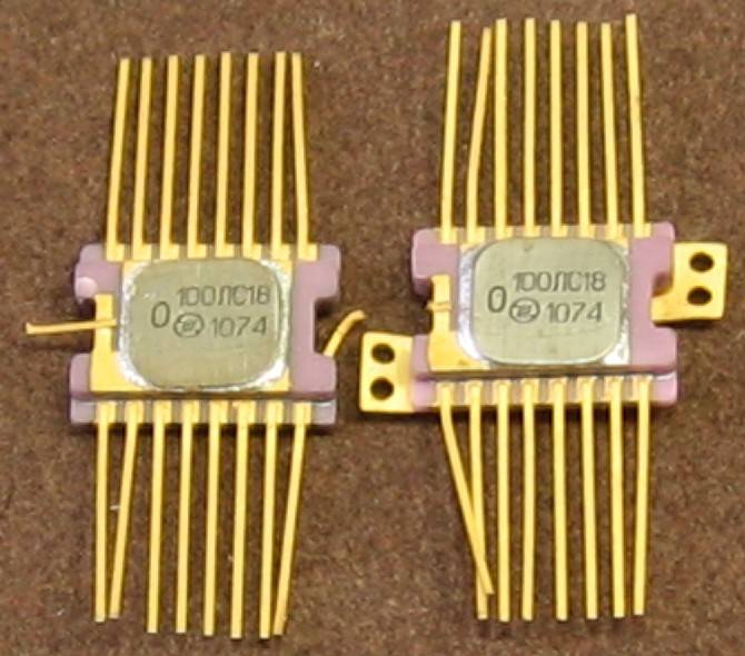
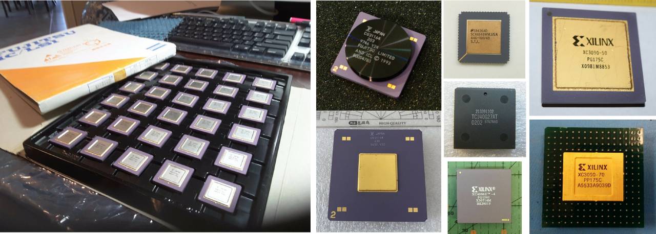
Here it is, the hundredth series, the basis of Elbrus-2
(https://1500py470.livejournal.com)
(https://1500py470.livejournal.com)
Further, the Yankees scored to improve the MC10000 technology, because a new MC10100 series appeared, and with it, as can be seen on the TEZ from the EU-1060, the copying process was difficult.
They managed to copy the K500TM130, but not yet the TM133, and with the MC10400 memory it turned out so badly that American chips had to be installed on serial machines in the first year of production.
The Americans have already released the MC10200 ...
In fact, the idea of the EU, as we have already said, was good in itself, and our designers did their best, let down the element base.
The Row-1 EU series as a whole was rather spoiled as a whole (due to poor manufacturing of civilian TTL), but the EU-1060 initially turned out to be just a disaster.
For example, in the same Research Institute "Delta" Melnikov preferred to do calculations for "Electronics SSBIS" according to the classics - on BESM-6, until their EU-1060 was replaced with the GDR EU-1055M, and Melnikov eventually retained his hatred for the EU for life.
However, the MEP got out easily - it released its own specifications, which did not coincide with the TX in those parameters that could not be met, and the 500 calmly passed the acceptance, using the unlimited patronage of the clone lord Shokin.
The matter ended with the fact that representatives of the Ministry of Defense (who also needed a powerful EU as a general-purpose computer, and not special air defense / missile defense computers) came directly to Shokin and expressed their official dissatisfaction with the following facts.
In the K500, as it turned out, there were no thermal compensating circuits at all, as a result of which the EC-1060 instantly warmed up to 70+ degrees, and this was the only way to ensure at least some operability, since it worked with uniform heating (albeit godlessly slowing down), and when uneven, it began to horribly fail due to desynchronization between colder and hotter ICs.
As a result, at the temperature range provided for by the governing documents of the Moscow Region, the microcircuits did not work, which was the subject of a complaint.
However, Shokin (who fell into an indescribable rage if he thought that someone dared to disagree with him) showed that the Ministry of Defense is not a decree for the MEP.
According to eyewitnesses, he explained in such a powerful peasant Great Russian language that the MEP produced the 500th series in full accordance with its specifications, and the TK from the Ministry of Defense can be sent straight and left, that even the military were shocked, and they retreated from the office.
As a result, the finally damned 100/500/700 series was only accepted by 1980 and at the same time cured her childhood sores.
Not surprisingly, one of Gorbachev's first decrees, with which he began to clear the Augean stables of Soviet ministries, was the decree on Shokin's resignation.
However, he did not have time to officially kick him out, he realized that he smelled fried, and preferred to leave a little earlier himself.
Actually, Burtsev also recalls this:
The Elbrus-2 MVK was built on a new element base.
This caused a lot of problems.
ICs turned out to be extremely unreliable: since they were copied, much was not copied, there were system errors.
We stood for a whole year, not knowing what to do, especially with memory.
MEP located the production of ICs at different factories, and I had to organize incoming control, because, for example, the Zelenograd schemes (the Mikron plant) worked perfectly, and the ICs produced in Kaunas had a case depressurization.
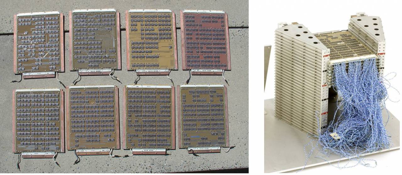
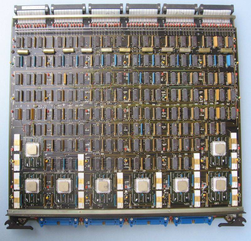
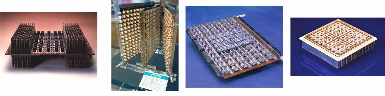
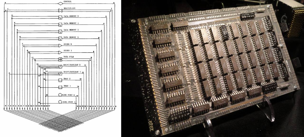
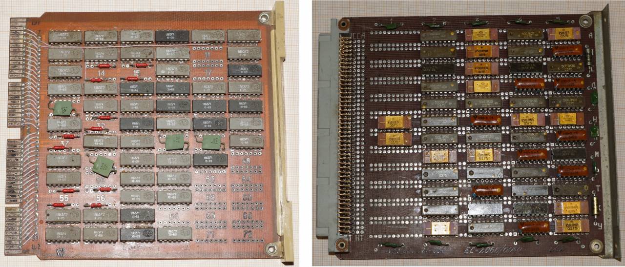
Boards from "Elbrus-2" of two generations. First, on the 100th series and K200 assemblies of 10 such crystals, and then on the BMK I200. Boards on display in Mountain View, California
(https://1500py470.livejournal.com)
(https://1500py470.livejournal.com)
The maximum problems awaited, as you might guess, with the K200 - an attempt to portray the Soviet MCM a la IBM 3081.
Many engineers who worked at ITMiVT considered Burtsev's decision to fuss with MBIS (multi-chip LSI, not to be confused with further MAIS - matrix LSI, i.e. BMK of the I200 series!) Completely erroneous and additionally delayed work on Elbrus-2.
The first K200s were ready in 1976, and development of the processor began.
Approximately half of its logic was implemented as individual 100-series chips, and the other half as K200 modules.
The packaging installation was made in ITMiVT itself, and it would be better if they did not do this ...
Debugging did not begin until 1981, according to one estimate, the reliability of the assemblies was such that something burned in the processor every time it was turned on and off.
Up to 5 TEZs were replaced per day, because of this, debugging took three times longer than planned.
In general, with TTL in Elbrus-1, the situation was not much better.
As a result, by 1984, the car was de jure handed over, de facto it was a prototype, which is still to be polished and polished (as we know, it was polished only by 1989, once again changing the element base, and it went into a full-fledged series only from 1990) .
As a result, Burtsev missed all conceivable deadlines for 10 years (despite the fact that ersatz-Elbrus, the first version on TTL, also worked normally no earlier than the beginning of the 1980s, and for such a wild infusion of money and anguish of strength, it turned out to be quite miserable).
This is what allowed Burtsev's ill-wishers to make a revolution in ITMiVT and, taking advantage of the fact that his mighty patron Kalmykov had been in the grave for 10 years, repeat over him the same thing that Burtsev did with Staros.
Even before the delivery of Elbrus-2, it became clear that, like its first version, it was hopelessly outdated technically.
The MC10k series looked good in 1970, but by 1985 it was already museum scrap metal.
As we have already mentioned, there were enough applicants for new technologies in the USSR.
Delta Research Institute - from the MEP side and ITMiVT with NICEVT - from the MRP side, while at the first stage all types of ECL were produced and developed only in Zelenograd at the MEP factories.
Information