Chronicles thermal imaging. Part of 2
The key problem of individual thermal imagers in the composition of the instrument-sighting complex are stringent requirements for mass and dimensions. Place the cooling system of the matrix with liquid nitrogen is impossible, so you have to look for new engineering solutions. But why bother to build the most complicated and expensive thermal imager, if you already have excellent infrared night vision devices for individual shooting? weapons? The matter is in masking the enemy, smoke, precipitation and light interference, all of which dramatically reduce the efficiency of night vision devices, even with third-generation electronic-optical converters. The product of the Novosibirsk TschB “Tochpribor” under the symbol 1PN116 is specifically designed to work in such conditions and is an old-school representative of devices for detecting infrared radiation of objects on the battlefield.
The 1PN116 thermal sight sees with its sharp-sighted vision everything the size of a person and that it is hotter than the natural background on 1200 meters ahead. The device has a significant mass (3,3 kg), and therefore put it mainly on the SVD, machine guns "Pecheneg" and "Kord". An uncooled microbolometer is used as a “retina”, the matrix of which has 320x240 pixels. We will understand more in the tricks of uncooled thermal imaging.
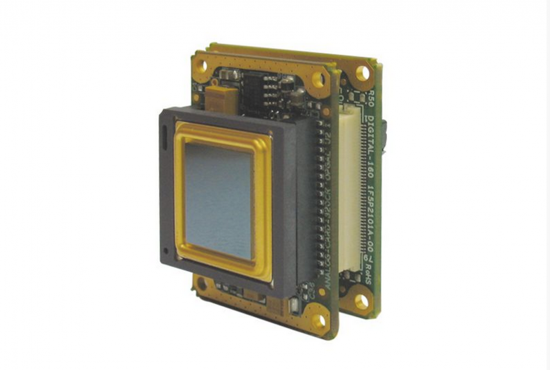
[Center]Military solid-state microbolometer
This is the third generation technology, which has fundamental differences from the previous ones by the absence of a complex and not always reliable optical-mechanical scanning system. In this generation, thermal imagers are based on Focal Plate Area (FPA) solid-state matrix receivers installed directly behind the plane of the lens. The “chemistry” of thermal vision in such gadgets, in the overwhelming majority of cases, is based on resistive layers of vanadium oxide VOx or amorphous silicon α-Si. But there are exceptions in which photodetectors or “hearts” of thermal imagers are based on PbSe, pyroelectric arrays of photodetectors, or matrices based on CdHgTe compounds equipped with thermoelectric cooling. Interestingly, such cooling is often not used for its intended purpose, but only provides thermal stability under varying environmental conditions. Microbolometers from the VOx or α-Si series register changes in electrical resistance under the influence of temperature, which is one of the basic principles of operation of a thermal imager. In each such solid-state sensor, there is a signal preprocessing chip that converts resistance into an output voltage and compensates for background radiation. An important requirement of a microbolometer is work in a vacuum and “heat-transparent” germanium optics, which seriously complicates the work of both designers and production workers. And the sensor itself must have a reliable substrate with inclusions of germanium or gallium arsenide. To understand all the details of the microbolometer's work, it should be noted that fluctuations in the crystal temperature on 0,1 K lead to a tiny change in resistance on 0,03%, which must be tracked. Amorphous silicon, with all other things being equal, has some advantages over vanadium oxides - the uniformity of the crystal lattice and high sensitivity. This makes the image more contrast to the user and less susceptible to noise, compared with similar technology on VOx. Each pixel of a microbolometer is unique in its own way - it has its own, slightly different from its fellows, gain and offset factors that affect the final image. By increasing the number of pixels, reducing the pitch between them (up to 9-12 microns) and miniaturizing them, the designers are trying, including reducing the noise level in the image. “Bad” or defective pixels are a serious problem in the manufacture of microbolometers, forcing engineers to develop software mechanisms for leveling white or black dots on the screen and flickering particles. Usually this is organized by means of interpolation, that is, the outgoing signal from the "broken" pixel is replaced with the derivative of the value of the neighbors. The most important parameter of the matrix is the value of NETD (Noise Equivalent Temperature Difference) or the temperature at which the microbolometer differs from the noise signal. Of course, the sensor should work quickly, so the next parameter is the time constant or the speed with which the imager responds to temperature changes. The fill factor or fill factor is a characteristic of the matrix that reflects the level of the microbolometer's sensitivity to sensitive elements; the larger it is, the better the image the operator sees. Hi-tech matrices can boast 90-% matrix filling with the number of pixels reaching 1 million. The user can observe the battlefield in two versions - a monochrome and color palette.
The developments of American scientists regarding the use of graphene as an infrared sensor look promising. This 2D material is not being tried anywhere, and now it is the turn of the thermal imaging technology. Given that 70-80% of the cost of an uncooled thermal imager is a microbolometer and germanium optics, the idea of creating graphene thermoelectric sensors is very tempting. According to the Americans, a single layer of relatively inexpensive graphene on a silicon nitride substrate is enough and the prototype already acquires the ability to distinguish a person at room temperature.
Both abroad and in Russia, great attention is paid to developments related to the athermalization of optical systems of thermal imagers, that is, resistance to changes in ambient temperatures. The lenses are used from chalcogenide materials - GeAsSe and GaSbSe, in which the refractive indices of the rays depend little on temperature. The company LPT and Murata Manufacturing have developed a method for obtaining such lenses by hot pressing followed by diamond turning of aspherical and hybrid lenses. In Russia, one of the few manufacturers of athermal lenses is OAO NPO GIPO - State Institute of Applied Optics, which is part of the holding company Shvabe. Oxygen-free glass, zinc and germanium selenides are used as lens material, and the body is made of high-strength aluminum alloy, which ultimately guarantees no distortion in the range from -400С to + 500С.

In Russia, besides the mentioned 1PN116 from the FSUE “TsKB Tochpribor” (or “Shvabe-Devices”), the much lighter thermal sight “Shahin” (TsNII Tsiklon OJSC) was adopted, named for “vigilance” in honor of the predatory falcon species , featuring the French Ulisse matrix with 160x120 pixels (or 640x480) and the range of recognition of the growth figure in 400-500 meters. In recent generations, the imported microbolometer has been replaced with a domestic model.
Next on the list: the PT3 thermal imaging sight from Novosibirsk's “Shvabe - defense and defense” with matrix resolution in 640X480 elements, weight in 0,69 kg and, which became the “gold standard”, the detection range of the growth figure in 1200 m. The pixel pitch of this sight is not outstanding indicator and is 25 μm, which forms a modest final image resolution. By the way, the holding organized the production of a hunting sight based on military development under the code PTZ-02. Another representative of the national design school is the Alpha TIGR thermal imaging sight from the Shvabe Photo Instrument division, which appears to be a monopolist, with a microbolometer receiver in the 7-14 μm range with a resolution of 384X288 pixels. In "TIGRE" the operator works with a monochromatic OLED microdisplay on 800x600 pixels, of which 768x576 are reserved for displaying a thermal image. An important difference from the earliest examples of Russian thermal sights is the increased duration of work by 30 minutes - now you can fight 4,5 hours in the IR range. Its modification "Alpha-PT-5" has a rare PbSe photoelectric receiver with electrical thermal stabilization. The universal PT-1 sight from NPO “NPZ” can be combined with many samples of small arms due to a special attachment and memory, in which ballistics and target grids are programmed for a wide range of weapons. Squeezing the eye muscle of the eyecup of the sight turns on the microdisplay, and unclenching turns off - this is the energy saving system implemented in the PT-1. American microbolometers are installed on a thermal imaging device for aiming and observing the Granit-E from MNPK Spectr. The equipment with “wide-polar” vision is represented by a company with a long name NF IFP SB RAS “KTP PM” under the symbol TB-4-50 and has a field of view 18 degrees on 13,6 degrees.
By the way, the company offers a range of three types of thermal imaging sights, TB-4, TB-4-50 and TB-4-100, equipped with a modern microprocessor for image processing based on the HPRSC (High Computing) architecture. A separate direction are the new Mowgli-2М thermal imaging sights under the symbol 1PN97М installed on the family of Strela-2М, Strela-3, Igla-1, Igla, Igla-S and newest types of MANPADS. Verba. Develop and collect sights on the St. Petersburg LOMO and they differ, of course, the huge detection range in 6000 m. TV / S-02 sights from BELOMO from neighboring countries can be an alternative to Mowgli for heavy rifles, rocket launchers and, actually, MANPADS. With a mass of no more than 2 kg, the Belarusian sight demonstrates an impressive detection range of a person in 2000 meters, and recognition in 1300 meters.
In this part of the Thermal Imaging Chronicles, we talked about some domestic thermal imaging individual sights and their counterparts from neighboring countries. Foreign analogues are ahead tank thermal imagers, as well as individual monitoring and intelligence devices.

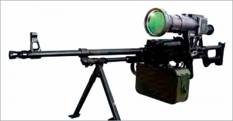
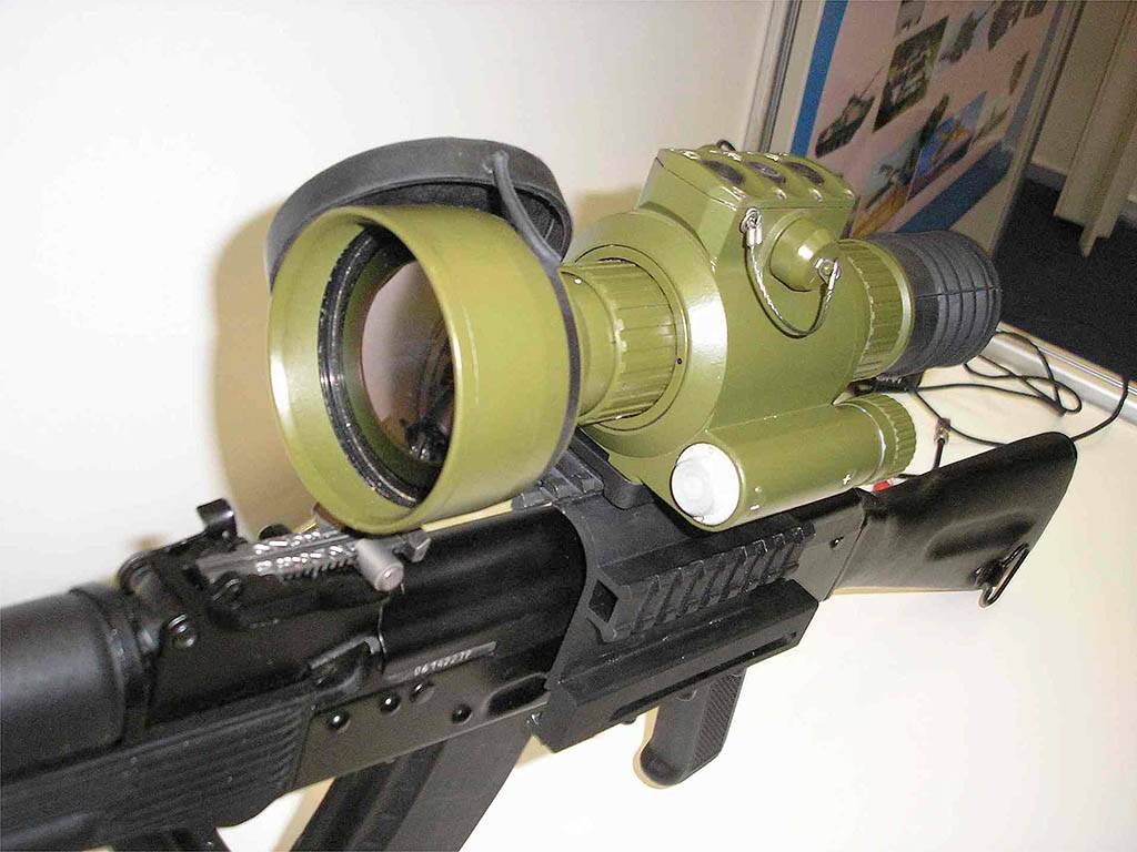
1PN116 installed on PCM
The 1PN116 thermal sight sees with its sharp-sighted vision everything the size of a person and that it is hotter than the natural background on 1200 meters ahead. The device has a significant mass (3,3 kg), and therefore put it mainly on the SVD, machine guns "Pecheneg" and "Kord". An uncooled microbolometer is used as a “retina”, the matrix of which has 320x240 pixels. We will understand more in the tricks of uncooled thermal imaging.

[Center]Military solid-state microbolometer
This is the third generation technology, which has fundamental differences from the previous ones by the absence of a complex and not always reliable optical-mechanical scanning system. In this generation, thermal imagers are based on Focal Plate Area (FPA) solid-state matrix receivers installed directly behind the plane of the lens. The “chemistry” of thermal vision in such gadgets, in the overwhelming majority of cases, is based on resistive layers of vanadium oxide VOx or amorphous silicon α-Si. But there are exceptions in which photodetectors or “hearts” of thermal imagers are based on PbSe, pyroelectric arrays of photodetectors, or matrices based on CdHgTe compounds equipped with thermoelectric cooling. Interestingly, such cooling is often not used for its intended purpose, but only provides thermal stability under varying environmental conditions. Microbolometers from the VOx or α-Si series register changes in electrical resistance under the influence of temperature, which is one of the basic principles of operation of a thermal imager. In each such solid-state sensor, there is a signal preprocessing chip that converts resistance into an output voltage and compensates for background radiation. An important requirement of a microbolometer is work in a vacuum and “heat-transparent” germanium optics, which seriously complicates the work of both designers and production workers. And the sensor itself must have a reliable substrate with inclusions of germanium or gallium arsenide. To understand all the details of the microbolometer's work, it should be noted that fluctuations in the crystal temperature on 0,1 K lead to a tiny change in resistance on 0,03%, which must be tracked. Amorphous silicon, with all other things being equal, has some advantages over vanadium oxides - the uniformity of the crystal lattice and high sensitivity. This makes the image more contrast to the user and less susceptible to noise, compared with similar technology on VOx. Each pixel of a microbolometer is unique in its own way - it has its own, slightly different from its fellows, gain and offset factors that affect the final image. By increasing the number of pixels, reducing the pitch between them (up to 9-12 microns) and miniaturizing them, the designers are trying, including reducing the noise level in the image. “Bad” or defective pixels are a serious problem in the manufacture of microbolometers, forcing engineers to develop software mechanisms for leveling white or black dots on the screen and flickering particles. Usually this is organized by means of interpolation, that is, the outgoing signal from the "broken" pixel is replaced with the derivative of the value of the neighbors. The most important parameter of the matrix is the value of NETD (Noise Equivalent Temperature Difference) or the temperature at which the microbolometer differs from the noise signal. Of course, the sensor should work quickly, so the next parameter is the time constant or the speed with which the imager responds to temperature changes. The fill factor or fill factor is a characteristic of the matrix that reflects the level of the microbolometer's sensitivity to sensitive elements; the larger it is, the better the image the operator sees. Hi-tech matrices can boast 90-% matrix filling with the number of pixels reaching 1 million. The user can observe the battlefield in two versions - a monochrome and color palette.
The developments of American scientists regarding the use of graphene as an infrared sensor look promising. This 2D material is not being tried anywhere, and now it is the turn of the thermal imaging technology. Given that 70-80% of the cost of an uncooled thermal imager is a microbolometer and germanium optics, the idea of creating graphene thermoelectric sensors is very tempting. According to the Americans, a single layer of relatively inexpensive graphene on a silicon nitride substrate is enough and the prototype already acquires the ability to distinguish a person at room temperature.
Both abroad and in Russia, great attention is paid to developments related to the athermalization of optical systems of thermal imagers, that is, resistance to changes in ambient temperatures. The lenses are used from chalcogenide materials - GeAsSe and GaSbSe, in which the refractive indices of the rays depend little on temperature. The company LPT and Murata Manufacturing have developed a method for obtaining such lenses by hot pressing followed by diamond turning of aspherical and hybrid lenses. In Russia, one of the few manufacturers of athermal lenses is OAO NPO GIPO - State Institute of Applied Optics, which is part of the holding company Shvabe. Oxygen-free glass, zinc and germanium selenides are used as lens material, and the body is made of high-strength aluminum alloy, which ultimately guarantees no distortion in the range from -400С to + 500С.
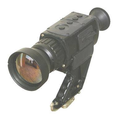
Thermal imaging sight "Shahin" from the Central Research Institute "Cyclone"
In Russia, besides the mentioned 1PN116 from the FSUE “TsKB Tochpribor” (or “Shvabe-Devices”), the much lighter thermal sight “Shahin” (TsNII Tsiklon OJSC) was adopted, named for “vigilance” in honor of the predatory falcon species , featuring the French Ulisse matrix with 160x120 pixels (or 640x480) and the range of recognition of the growth figure in 400-500 meters. In recent generations, the imported microbolometer has been replaced with a domestic model.
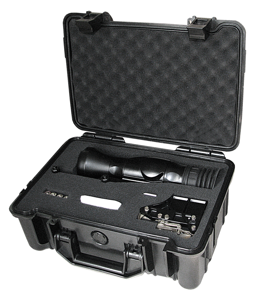
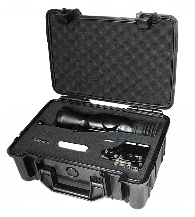
PT3 thermal sight stored in a case
Next on the list: the PT3 thermal imaging sight from Novosibirsk's “Shvabe - defense and defense” with matrix resolution in 640X480 elements, weight in 0,69 kg and, which became the “gold standard”, the detection range of the growth figure in 1200 m. The pixel pitch of this sight is not outstanding indicator and is 25 μm, which forms a modest final image resolution. By the way, the holding organized the production of a hunting sight based on military development under the code PTZ-02. Another representative of the national design school is the Alpha TIGR thermal imaging sight from the Shvabe Photo Instrument division, which appears to be a monopolist, with a microbolometer receiver in the 7-14 μm range with a resolution of 384X288 pixels. In "TIGRE" the operator works with a monochromatic OLED microdisplay on 800x600 pixels, of which 768x576 are reserved for displaying a thermal image. An important difference from the earliest examples of Russian thermal sights is the increased duration of work by 30 minutes - now you can fight 4,5 hours in the IR range. Its modification "Alpha-PT-5" has a rare PbSe photoelectric receiver with electrical thermal stabilization. The universal PT-1 sight from NPO “NPZ” can be combined with many samples of small arms due to a special attachment and memory, in which ballistics and target grids are programmed for a wide range of weapons. Squeezing the eye muscle of the eyecup of the sight turns on the microdisplay, and unclenching turns off - this is the energy saving system implemented in the PT-1. American microbolometers are installed on a thermal imaging device for aiming and observing the Granit-E from MNPK Spectr. The equipment with “wide-polar” vision is represented by a company with a long name NF IFP SB RAS “KTP PM” under the symbol TB-4-50 and has a field of view 18 degrees on 13,6 degrees.
Thermal Sight TB-4-100
By the way, the company offers a range of three types of thermal imaging sights, TB-4, TB-4-50 and TB-4-100, equipped with a modern microprocessor for image processing based on the HPRSC (High Computing) architecture. A separate direction are the new Mowgli-2М thermal imaging sights under the symbol 1PN97М installed on the family of Strela-2М, Strela-3, Igla-1, Igla, Igla-S and newest types of MANPADS. Verba. Develop and collect sights on the St. Petersburg LOMO and they differ, of course, the huge detection range in 6000 m. TV / S-02 sights from BELOMO from neighboring countries can be an alternative to Mowgli for heavy rifles, rocket launchers and, actually, MANPADS. With a mass of no more than 2 kg, the Belarusian sight demonstrates an impressive detection range of a person in 2000 meters, and recognition in 1300 meters.
In this part of the Thermal Imaging Chronicles, we talked about some domestic thermal imaging individual sights and their counterparts from neighboring countries. Foreign analogues are ahead tank thermal imagers, as well as individual monitoring and intelligence devices.
Information