Alpha lithograph: Russia is learning to produce semiconductors
Critical technology
A little background to understand the situation in which modern Russian microelectronics production finds itself.
Now the country is ready to produce, more or less efficiently, only microchips with a 90 nm topology. Production is based at Zelenograd Micron and operates at the limit of its capabilities. It's all about imported photolithographic equipment, which you have to maintain and repair on your own. Equipment for “printing” microcircuits is produced by a few companies in the world, and it is very easy for Americans to monitor the traffic of scarce components.
By the way, with the start of the special operation, a total ban on the supply of photolithographic equipment to Russia became a logical continuation of many years of restrictions. In order for the Americans to allow the Dutch ASML or, at worst, the Japanese Nikon to sell equipment to Russia, it was probably necessary to place the second Rammstein in the Moscow region. And transfer the entire nuclear stockpile of the country into the hands of the Pentagon. South Korea, for example, took exactly this path. Taiwan was dealt with without military bases, but vassal dependence on American supplies was sufficient. weapons and the close proximity of the Seventh fleet USA.
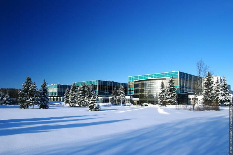
When the last Nikon and ASML lithographs fail at Zelenograd Micron, there will be nowhere to produce semiconductors.
That is why the largest manufacturers of modern microchips are concentrated in Korea, Taiwan and the United States. Washington keeps lithography technologies more than nuclear secrets - there are far fewer states capable of producing equipment for the microelectronics industry than there are owners of the most powerful weapons in the world.
If we take the most complex 7nm photolithography process as a starting point, then only ASML (Netherlands) and Nikon (Japan) can offer such machines. Moreover, the Japanese have very big reservations.
In Russia, as mentioned above, technology can only produce 90 nm chips and only on imported equipment. According to scientists from the Institute of Physics of Microstructures of the Russian Academy of Sciences, domestic technologies lag behind world technologies in lithography resolution by an order of magnitude, and in the density of a two-dimensional pattern on a chip - by two orders of magnitude. This is such a sad statistic.
As ethereal dreams, what would have happened to Russian lithography if the microelectronics industry, and not Rusnano, had received 280 billion rubles at one time?
Now the government intends to allocate 2025 billion rubles by 100 for the development of a full cycle of semiconductor production. This is frankly not enough - the annual budget of the Dutch ASML exceeds 3,35 billion euros.
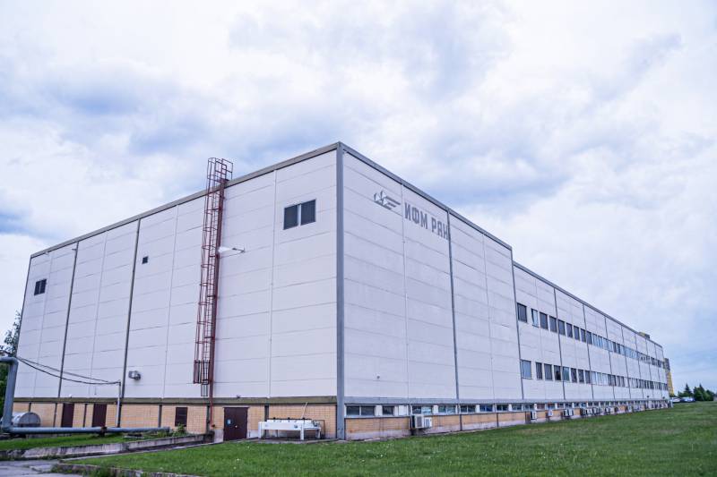
The Institute of Physics of Microstructures of the Russian Academy of Sciences should become the lead developer of the domestic photolithograph. Source: olympiada.scientificrussia.ru
The depth of the crisis is revealed by comparing the situation with other industries in which there has been a lag.
For example, the aircraft industry, which came under strict sanctions. Now the industry is able, albeit with great reservations, to produce aircraft for domestic airlines. They may be outdated and not the most economical (for example, the Tu-214), but they can operate in the sky, transport cargo and passengers. The situation is similar in the automotive industry.
But there is a real crisis in microelectronics - even with the ancient 130-nm topology, chips are built on imported sanctioned technology. The age of foreign machine tools is, of course, short-lived.
Part of the problem can be solved by diplomatic mail, stuffing parcels from Europe and the USA with scarce microcircuits and chips, but this is a temporary measure. China looms on the horizon with its permanent technological revolution. But Beijing will never, ever supply photolithographs to Russia. Firstly, this is a powerful tool of influence on Moscow, and secondly, the Chinese themselves do not yet have a normal production of machines for chips.
Let's try to figure out what stage of development the domestic base for photolithography is at.
Second atomic project
For a domestic scientist, engineer and technologist, nothing is impossible. And this is without unnecessary pathos - just remember the nuclear and space projects of the Soviet Union. A country with constantly catching up technological development was able not only to stand on par with the world hegemons, but also to get ahead for years. You just need to find the right managers with strategic thinking. We will find out in the coming years whether we have managed to find effective managers now, when Russia will or will not have its own microelectronics.
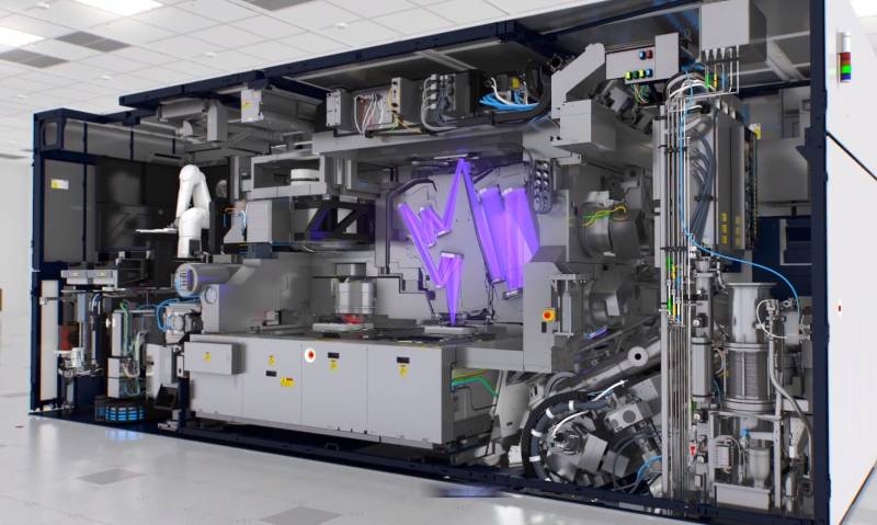
Even an extremely simplified diagram of the operation of an X-ray photolithograph clearly shows the level of complexity of the product.
In the meantime, we can only rely on specialists from the Institute of Physics of Microstructures of the Russian Academy of Sciences, or more precisely, the department of multilayer X-ray optics.
Despite the long-term lack of interest on the part of the state in the problem of sovereign lithography, the institute has some developments. For example, ultra-precise X-ray optics on ruthenium-beryllium mirrors. To understand the importance: Zeiss built an entire special optics plant specifically for the needs of the Dutch ASML. They claim that they will learn how to make mirrors for 7-8 nm photolithographs, and this task is not much simpler than launching a man to the Moon. The size of the roughness on the mirror must be less than one nanometer, otherwise the X-ray wave will be reflected with aberrations and story It won't burn out with chips.
Currently, the Russian institute is working on an X-ray lithograph, which, according to scientists, will be 1,5 times more efficient than imported analogues. This is a very bold statement, but the optimism of scientists cannot but rejoice. At the first stage, it is planned to create a schematic diagram of X-ray lithography in metal and plastic and a so-called alpha machine or technology demonstrator.
The unit will not be able to mass-produce microchips, but it will be able to demonstrate the possibility. At least two years are allocated for this. The chip topology is expected to be 28–32 nm in size. And this is only for extremely favorable conditions.
The fact is that management decisions and abundant funding are not a panacea for eliminating the backlog. We need highly qualified personnel, which is a problem. Low salaries have been washing away specialists from all scientific fields without exception for decades. Security Council Secretary Nikolai Patrushev recently reminded everyone that over the past twenty years the number of scientists has decreased by a quarter! According to him,
There is a time bomb buried here - in the near future there may simply not be enough brains to storm the lithographic peaks. Even if it is now possible to create a sufficient personnel training system, the first specialists will appear no earlier than in ten to fifteen years. By that time, photolithographs may no longer be needed at all.
Let's not talk about sad things.
In four years, a beta machine or industrial prototype for the production of 28 nm chips should appear at the Institute of Microstructure Physics of the Russian Academy of Sciences. The first serial photolithographs are promised by 2030.
All of the above refers to the most high-tech units for Russia. They also plan to build equipment that is somewhat simpler to implement. Moreover, 65–350 nm chips will be much more in demand in the domestic industry. Primarily for the defense complex.
According to Deputy Head of the Ministry of Industry and Trade Vasily Shpak, in 2026 Russia will produce the first 130-nm chips using its own equipment. And next year, 2024, 350 nm semiconductors. The official is full of optimism, but we agreed to do without sadness for now. Let's save criticism for the first announcement about the shift of deadlines to the right, which is often observed in Russia.
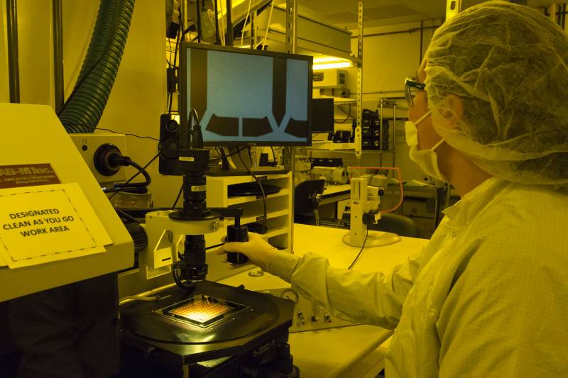
Can only be called a miracle news from St. Petersburg Polytechnic University.
Local engineers have come up with a kind of maskless mode for etching microcircuits, which is not inferior in quality to the best foreign models. In terms of price, it is generally cheaper by several decades - a Russian unit should cost up to 5 million rubles, and foreign ones cost 10–15 billion. Even if this is close to reality, there are enough nuances.
The breakthrough technology exists at the laboratory level and will require several years of complex engineering before it can be transformed into a working prototype. Or it won’t turn into anything at all - this has happened before, and not only in Russia.
The revival associated with the development of 100 billion rubles provided for by the state program for microelectronics is obvious. If a number of conditions are met and realistic deadlines are set, the history of the domestic photolithograph may turn out to be a reality.
You just need to find the right manager who can take on such responsibility. So far, unfortunately, no new Kurchatovs, Morozovs and Korolevs are on the horizon.
Information