In the defense industry developed a new radio-electronic equipment for aviation and space technology

94
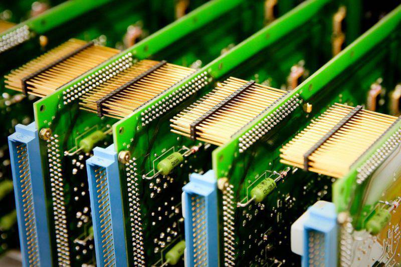
The United Instrument Engineering Corporation has completed work on creating samples of high-density radio-electronic equipment for airplanes and space rockets, which is able to work under extreme conditions and consume less energy compared to existing analogues, reports RIA News message of the press service of the company.


“OPK has created and successfully tested the first samples of high-density radio electronics of a new generation, including digital, power and microwave modules. Products built on 3-DMS technology of volumetric assembly have no analogues in Russia and surpass foreign samples in a number of technical characteristics. Modules are manufactured using unpackaged components. This greatly reduces the weight and dimensions of the products, allowing you to significantly expand the capabilities of the equipment. The novelty of technical solutions is confirmed by patents of the Russian Federation ", - stated in the release.

“The new technology will significantly improve the reliability of equipment operating in extreme conditions - on water, in the air, in space, in the regions of the Arctic or the Far North. Using 3-DMS technology allows you to reduce the size and weight of products by 4-8 times. At the same time, its performance characteristics are improved and energy consumption is reduced. First of all, such high requirements are relevant for equipment delivered in the interests of the space industry, aviation and naval fleet»
The press service cites the words of the director of the information development department, Alexander Kalinin

It is reported that "3-DMS technology is planned to be used in the production of new communication equipment, automated control systems, computing systems, robotics, unmanned aerial vehicles."

“Due to the unique design and improved characteristics, the modules can be used in various types of electronic equipment, in fault-tolerant on-board systems of airplanes and spacecraft. In particular, they can be equipped with Doppler meters for speed, angle of demolition and height (DISS-MLK) used in civilian and military aviation and rocket technology, ”the release notes.
94 comments
Information
Dear reader, to leave comments on the publication, you must sign in.
  1. +8
    14 January 2016 17: 35
    Well .. and who said that Russian microcircuits are the largest microcircuits in the world? smile We can if we want fellow
    1. +4
      14 January 2016 17: 44
      We can if we want

      Yes, we always could and can.
      The question is who needs this?
      If the military needs it, we immediately give it to the mountain!
      And the others apparently do not need. Prefer to buy Anostrannoe smile
      1. +4
        14 January 2016 18: 28
        I read it as if it weren’t for military developments, now we wouldn’t have mobile phones either. So, as they say, there is a plus in any minus, and minus in any plus hi
        1. +3
          14 January 2016 20: 28
          Quote: Dr. Bormental
          I read it as if it weren’t for military developments, now we wouldn’t have mobile phones either. So, as they say, there is a plus in any minus, and minus in any plus hi

          For the first time in the world, mobile phones were created by Soviet developers and not at all for war, but for top officials of the state so that there is constant communication even when traveling in a car.
          But the communication system, i.e. information transfer between cell stations, came up with a German woman (engineer) immediately after the war, after emigrating to the United States.

          The military has nothing to do with it.
          1. +6
            14 January 2016 20: 40
            Quote: Алексей_К
            The military has nothing to do with it.

            .. how to say, how to say .. here is another very interesting news that was almost imperceptible ..
            Scientists from the Laboratory of Nanophotonics and Metamaterials of ITMO University have experimentally confirmed the possibility of creating an optical analog of a conventional semiconductor transistor based on just one silicon nanoparticle. The results of the work can be further used in the development of optical computers, where transistors must have the ability of ultrafast switching and increased compactness. The study of scientists was published in the highly rated scientific journal Nano Letters.
            The performance of modern computers, in which electrons act as a signal carrier, is largely limited by the switching time of the transistor - of the order of 0.1–1 nanoseconds (10–9 seconds). It is assumed that in optical computers, the signal carried by photons will be able to accommodate much more information than a standard electrical signal. For this reason, the development of optical computers is impossible without the creation of an ultrafast optical transistor, that is, a miniature device that will manage to control the passage of a useful light signal due to an external control signal within a few picoseconds (10-12 seconds).
            In the work is a group of Russian scientists from ITMO University, Physics Institute. P.N. Lebedev Russian Academy of Sciences and the Academic University in St. Petersburg proposed a conceptually new approach to the development of such a transistor, making it a prototype of only one silicon nanoparticle.
            Our concept is different in that we propose to control not the absorption, but the radiation pattern of the particle. In other words, in normal mode, a particle, for example, scatters almost all of the light backward, but as soon as the particle receives a more intense control signal, it starts to rebuild and scatter forward.
            The choice of silicon as the material for the transistor was not accidental. The implementation of an optical transistor requires the use of low-cost materials suitable for mass production and capable of changing their optical properties in a few picoseconds (in the dense electron-hole plasma mode) and almost not being heated.
            “The switching time between the operating modes of our nanoparticle is only a few picoseconds, and we bring it into operation mode for tens of femtoseconds (10-15 seconds). Now we already have preliminary experimental data in our hands, indicating that the particle can successfully play the role optical transistor. Now we plan to conduct experiments where along with the control laser beam there will also be a useful signal beam, ”concludes the article’s co-author, head of the nanophotonics and metamaterials laboratory Pavel Belov.
            Source: http: //professionali.ru/Soobschestva/promyshlennost/sverhbystryj-optich
            eskij-tranzistor /
            .. hi
      2. +1
        14 January 2016 22: 34
        Prefer to buy Anostrannoe


        They do not prefer, but nowhere to go. For the same DISS mentioned, a citizen will need ARINC chips - again, please bow to the Americans. Do you want a microcontroller and enter the market - it’s so certified for aviation with a Texas instrument and cheaper and the widest choice. For yourself, sculpt what you want. And to them to the market - figs.
        1. 0
          14 January 2016 22: 57
          Sorry, "Angstrem" has finally blinded an analogue for the 429th smile Are born, dear. I was looking for two years ago, there wasn’t a damn thing.
    2. +2
      14 January 2016 17: 45
      Thanks to its unique design and improved performance ......
      - I am glad that NATO guys read this. And slowly they begin to understand that you can’t take Russia in a snap.
    3. +4
      14 January 2016 17: 46
      OPK created and successfully tested the first samples of high-density radio electronics of a new generation

      what
      Coincidence... winked
    4. +6
      14 January 2016 17: 47
      “OPK created and successfully tested the first samples of high-density radio electronics of a new generation

      It remains to work out the industrial technology ...
      1. +4
        14 January 2016 17: 51
        Quote: NIKNN
        It remains to work out the industrial technology ..

        It remains for such super-reliable electronics to really massively introduce. In the same flight recorders, so as not to disgrace the whole world, as with that "black box" Su-24.
    5. +4
      14 January 2016 18: 36
      Quote: Dr. Bormental
      We can if we want

      Uh ... I understand that everyone knows what 3-DMS is. Would they have enlightened ... The web is silent on this request like a fish on ice ... There is DMS technology (Direct Metal Sintering - Direct sintering of metals), but it seems that something else was meant here ... The photo is certainly beautiful - a few boards not connected anywhere (it looks like TEZs), but about nothing ...

      PS If only this: "high density multilayer hybrid integrated circuits (3D-GIS, 3-DMS), three-dimensional circuits on plastics (3D-MID), high-density printed circuit boards with built-in flexible-rigid components", but again about the technology solid fog ...
      1. +6
        14 January 2016 18: 49
        And then I ... why immediately? I am a doctor. Do you want to tell about appendicitis? feel
      2. The comment was deleted.
      3. 0
        15 January 2016 13: 28
        Little information. From what it is, let me suppose that by 3-DMS technology we mean a software product: a set of applications connected by common formats, providing a complete production cycle for bulk RE modules.
        The developer in one application designs / simulates the operation of the device, draws a diagram, transfers the file to the manufacturers.
        They automatically develop volumetric installation of module elements (in this volumetric wiring of the board there is novelty).
        Next is the production site, where the device comes to life (not without the help of 3-D printers).
        1. 0
          15 January 2016 14: 41
          Is it really that everyone is really so limited that they cannot understand that the magnetic fluxes in each electronic device can work in coordination with other devices, and hence the volumetric format appears, when it is possible not to design circuits and contours with boards in the plane, but in the volume of system coordinates. At the same time, I am sure that designers should have ideas in which direction to design these electronic devices. For example, the same Villari effect can be used with great success in a transformer, which can be derived from the interpretation of the effect itself. The transistor, for example, is not in linear polarization, but in bulk. But the most amazing thing is that this is just the beginning. Since magnetic fluxes can and should be used in electronic devices not as a derivative of a pronounced increase in temperature. and the derivatives at the moment of rotation. Then .... In general, "born to crawl will not be able to fly" This is not personal to you. If a country wants to be strong and rich, then talented people need to be given the opportunity for self-realization. People need to look for !!! And use the talents of everyone. I'm not talking about myself.
          1. 0
            15 January 2016 16: 37
            Yes ... You, a colleague, are clearly not in the subject, but you write them down to limited ones.
            To get started, read this at least 2008 article: www.electronics.ru/files/article_pdf/0/article_372_114.pdf
            There we are talking about three-dimensional multi-chip modules, the key role of computer-aided design systems in their development and production, which I wrote to my comrades in the previous comment in an accessible form.
            1. 0
              15 January 2016 16: 57
              If you read this article, you will understand that nothing particularly breakthrough has happened, it is just that Vega has finally implemented the described technology into real production hi
              1. 0
                15 January 2016 18: 26
                Thanks for the link. All this is primitive. We are talking about systems that do not need at all, we will say, support or substrate. That is, as in any living body. Each part is a system participant in the process. The elemental base and essence of the compounds themselves is organized completely differently. If we distract ourselves from theory, then electrical connections made in a linear fashion, i.e., as a connection with a segment of a linear conductor, are not the best way. Because magnetic force processes and their gradient like electricity are spatial formations. Moreover, in the nature of el. processes induction devices, namely those that perform a similar function do not have the form of spirals. Is this not to know any attentive person. And much more.
                1. 0
                  15 January 2016 23: 51
                  Thanks for the reply.
                  You are ahead of thought by much (if you do not bother laughing ) progress.
                  Not everyone is given, of course.
                  I am glad: thank God, we really got to the realization of simple things applicable in the production, even if in your opinion primitive, but it works, strengthens the country's defense power.
                  Next: it's up to science. And by you. Move it, science.
    6. 0
      14 January 2016 18: 41
      Quote: Dr. Bormental
      Well .. and who said that Russian microcircuits are the largest microcircuits in the world?

      and where did you get the idea that they are not the biggest?
      Quote: Author
      Using 3-DMS technology allows reduce the dimensions and weight of products by 4-8 times.

      Quote: Author
      not have analogues in Russia and a number of technical Features superior to foreign designs.

      ...
      honestly, for a long, long time poking around.
      There are no details of "3DMS Technology" (neither we, nor they).
      TECHNOLOGY OF PRODUCTION OF HIGH-DENSITY ELECTRONIC MODULES (from JSC Concern Vega)?
      So this is "a method of group mounting crystals when assembling high-density electronic modules - intended for use in the assembly process three-dimensional multi-chip electronic modules during the installation of shell-less crystals in the volume of a micro-switching board


      Development of a basic technology for the integration of 3D microcircuits for the production of promising electronics products. Technical project OKR "Installation 3D", P.6. OJSC Concern Vega.


      All over the world this is called: three-dimensional integration with through holes through cream-
      Niy (Through-Silicon-Vias, TSV). 3D-TSV

      The Sematech Consortium launched a 2005D interconnection program in 3
      program). GlobalFoundries, UMC, are involved in the implementation of the 3D Sematech program.
      HP, IBM, Intel, Samsung, ASE, Altera, Analog Devices, LSI, On Semiconductor, Qualcomm. In August 2010, Sematech announced the commissioning of a line for the production of prototype 3D devices on 300 mm wafers at the Albany Nanotechnology Complex, part of the Nanoscale Science and Engineering, CNSE. The line is equipped with installations for the formation of through holes with a diameter of up to 5 microns and a depth of up to 50 microns, combining plates and crystals, weld conclusions, thinning the plates and making the necessary measurements.

      Quote: Author
      reduce the dimensions and weight of products by 4-8 times.

      Yes?
      - there are contact pads on the microcircuit to which the microcircuit pins are connected - there is nowhere to reduce them, and therefore, if the microcircuit area is comparable to the area of ​​the contact pads - then making the microcircuit using more sophisticated technology also makes no sense
      - there are hundreds of semiconductor devices on the ISS circuit - MOSFETs, drivers, power microcircuits, every minor trifle - almost all of them have enough 1000nm technology
      - All industrial electronics, and microcircuits for space and military - this is almost 100% of 180nm technology and thicker.

      Quote: Author
      Features superior to foreign designs.

      Oh well...
      A micron spanks 3000 plates a month - it covers volumes with your head Metro and defense tickets

      The supplier of basic technology 180 and 90nm is the French company STMicroelectronics. Further modifications of the technology are already done at Micron (for example, SiGe, silicon-on-insulator, etc.). The equipment is also imported.
      Photo masks for critical layers (with the smallest details) have to be made abroad.
      1. 0
        14 January 2016 18: 47
        I did not understand anything from what you wrote. Can you write a resume from all these technical calculations?
        1. +1
          14 January 2016 19: 04
          Quote: Dr. Bormental
          I did not understand anything from what you wrote. Can you write a resume from all these technical calculations?

          They called the well-known technology in their own way, let them in the fog ... It's like appendicitis in Latin ... Of course, better than nothing.
          1. -1
            14 January 2016 19: 50
            Quote: region58

            Well-known technology was called in its own way.

            Famous?
            Well, enlighten, please.
            Quote: opus
            There are no details of "3DMS Technology" (neither we, nor they).

            Quote: opus
            OKR "Installation 3D", clause 6. OJSC Concern Vega.


            Quote: region58
            There is a technology DMS (Direct Metal Sintering - Direct sintering of metals)

            Yeah fool
            Or in the 58th region it is customary only to scratch the tongue, but to mock it?
            1. +1
              14 January 2016 20: 24
              Quote: opus
              Or in the 58th region it is customary only to scratch the tongue, but to mock it?

              I apologize, have I offended you with something ??? I didn’t understand about the jokes ... Out of the blue it came ... Deliciously spat in the soul ... And as for the technology - so you explained what was what.
              1. +1
                14 January 2016 21: 01
                Quote: region58
                Out of the blue it flew ...

                my fault. do not perceive.
                when you do a lot of things, you are stupid (like me) and you answer the wrong way.
                It was too late to delete .... the timing of the TV is very small
                Do you want + put as an apology request
                Honestly: it was not written to you (about the slander)
                1. +1
                  14 January 2016 21: 06
                  Quote: opus
                  my fault. do not perceive.
                  when you do a lot of things, you are stupid (like me) and you answer the wrong way.
                  It was too late to delete .... the timing of the TV is very small
                  Do you want + I will put as an apology request
                  Honestly: it was not written to you (about the slander)

                  Yes, I already realized that something is not right ... accepted ... it happens ... Pluses are not necessary - happiness is not in them ...
        2. +1
          14 January 2016 20: 09
          Quote: Dr. Bormental
          Can you write a resume from all these technical calculations?

          so this and so the resume.
          All write-articles are not enough.
          Well, P:
          -something I hardly believe (another "one who has no analogue in the world"
          or zhurnalyug stupid.
          I do not know.
          But our chips are the BIGGEST in the world. for sure
          -------------------------------------------------- ---
          It is about three-dimensional integration. This is a technology that allows you to create systems with a high degree of integration, by vertically stacking and joining various layers, in particular, semiconductor crystals.


          For example: you can take a DRAM crystal and place it on top of the microprocessor chip.

          More clearly = you can live like this or like this:

          which is more sociable and compact?

          -----------------------------
          The world's first microprocessor manufactured to this standard (3D) was the chip, codenamed Ivy Bridge on the Tri-Gate tr-re

          The stages were as follows:

          it was so awesome.
          Yes, we did not even reach 2002.


          Last squeak (for today) - 3d TSV (through-silicon via)

          characterized by the presence of through joints between the layers at an arbitrary point.


          ----------------
          So I don’t understand what our "did" this


          Quote: opus
          "3DMS technology" - no where (neither we, nor they).

          but obviously not
          Quote: region58
          Direct sintering of metals
          ?
          belay
          Or no
          Quote: region58
          appendicitis

          ?
          1. 0
            14 January 2016 20: 13
            Quote: opus
            ?

            Well this is in response to
            Quote: opus
            I am a doctor. Do you want to tell about appendicitis?

            Just kidding ...
            1. +1
              14 January 2016 21: 13
              Quote: region58
              So I don’t understand what our "did" this

              Everything is clear in the article, albeit very briefly.
              This "last squeak (for today) - 3d TSV (through-silicon via)" is just the manufacture of a microcircuit (from elements of the same type) not on a large crystal plane, but by racking it into several planes with their subsequent volumetric electrical connection.
              The article states that:
              "" The OPK has created and successfully tested the first samples of high-density radio electronics of a new generation, including digital, power and microwave modules. Products built using the 3-DMS volume assembly technology have no analogues in Russia and surpass foreign models in a number of technical characteristics. Modules are manufactured using a frameless element base. This significantly reduces the weight and dimensions of products, allowing you to significantly expand the capabilities of the equipment. The novelty of technical solutions is confirmed by patents of the Russian Federation. ”
              This is not a microcircuit, but a huge microelectrocircuit of whole blocks of radio equipment, consisting of many very different unpackaged microradioelements. A simple chip is far from such microminiaturization.
          2. 0
            15 January 2016 12: 39
            Create such a sandwich - well done! Only the question arises of heat dissipation and overheating of such solutions.
        3. 0
          14 January 2016 20: 54
          Quote: Dr. Bormental
          I did not understand anything from what you wrote. Can you write a resume from all these technical calculations?

          Of course it’s not clear, you didn’t learn this and you weren’t a radio amateur either.

          But from the field of radiochemistry, a phrase from the dissertation:
          "In radiochemical practice, actinides are most often isolated from saline solutions of complex composition. Therefore, we have studied the extraction of Am (III) from a 03M solution of HN0,1-simulator BAO containing: U (VI) - 0,03; Pu (IV) - 10; Na (I) - 1; Ca (II) - 7,5; Al (III) - 2,5; Fe (III) - 2,5; Ni (II) -33; VP1 (0,5IÍ) - 10 g It was found that a solution containing 4-2 g-mol of Ph2Bu10 quantitatively extracts Ash (III) in 03 min. Therefore, the adduct formed during extraction is an effective extractant that extracts Am (III) from HNXNUMX solutions with a high salt content . "
          Do you understand much?

          What to do, you have to believe in the word that this is possible.

          And about the 3-DMS technology, it’s just a three-dimensional installation (microassembly) of many microradio elements not on a flat printed circuit board, but on a chip, on which only microcircuits were usually made. Moreover, it is also a volumetric installation of several such complex microassemblies.
          1. 0
            15 January 2016 00: 33
            I’m not vindictive, but I remember that when I talked about volumetric circuitry and element base with super high density of magnetic force flows, I was sent to vocational school to study. But this is in the past. Nevertheless, the principles of modeling volumetric devices remain old, since there is no element base that would allow such structures to be created. But!!! It is impossible to create and even imagine such an elemental base without the ability to manipulate the spatial modeling of magnetic force processes. To all this, it directly depends on the multi-valued logic of reasoning. All the same, everyone goes to what is called truth and is optimal and effective.
          2. -1
            15 January 2016 11: 21
            The first subconscious conclusion was, as always, correct: "He is a ram, not in form, but in essence."
      2. The comment was deleted.
      3. +1
        14 January 2016 18: 57
        Quote: opus
        All over the world this is called: three-dimensional integration with through holes through cream-
        Niy (Through-Silicon-Vias, TSV). 3D-TSV

        Wow! Respect. And then I broke my whole head, what kind of beast is this - 3-DMS.
        1. +1
          14 January 2016 20: 15
          Quote: region58
          Wow! Respect.

          first m / a by the way they replenished me with mud. Plentifully so, and even an appendicitis wink
          1. 0
            14 January 2016 20: 30
            Quote: opus
            first m / a by the way they replenished me with mud. Plentifully so, and even an appendicitis

            ???? I would venture to suggest that you did not look at the time of writing the comments ... and to whom they were written ...
          2. 0
            15 January 2016 00: 36
            ABOUT! I respected you completely in solidarity. How many times have I told myself that damn that day when I was driven by a desire to share my discoveries. It turns out that someone thinks the same way. And although they are still far from progress, it is still good.
      4. 0
        14 January 2016 19: 12
        Quote: opus
        All industrial electronics, and microcircuits for space and the military - this is almost 100% of technology 180nm thicker.

        However! If your computer has an AMD processor, then it uses 50-100nm technology. And if YOU have an advanced INTEL, then 20nm. Feel the difference in functionality and computing power with very small sizes, compared to 180nm and even more so 1000nm. Here is such an entertaining geometry. It is vitally important for us to master and introduce microelectronics of such nanoscale into at least into military production. The future lies with her.
        And when I hear or read in the text the phrase "has no analogues in ...." I immediately have vague doubts.
        1. +4
          14 January 2016 19: 21
          Quote: GSH-18
          If your computer has an AMD processor, then it uses 50-100nm technology. And if YOU have an advanced INTEL, then 20nm. Feel the difference in functionality and computing power with very small sizes, compared to 180nm and even more so 1000nm.

          What about reliability and resistance to all kinds of bad fields and radiation? The left gamma particle and the cranks flew to the 18-nm processor - it will get into a stupor, which will not happen at 180 nm.
          PS
          Engineers have created miniature electronic radio tubes that combine the properties of vacuum tubes and silicon transistors. It is planned that they will be able to become the basis of fast and radiation-resistant computing devices.
          According to the creators, the miniature lamp was able to work at frequencies of 0,46 terahertz, which is 10 times more than the maximum frequency of the best silicon transistors. It is characteristic that for its operation it was not necessary to create a vacuum in the cavity — the lamp was so small that it made the probability of an electron meeting a gas molecule in the path between the cathode and anode extremely low.

          so the lamp processor may not be a joke ... recourse
          1. -3
            14 January 2016 19: 34
            Quote: region58
            What about reliability and resistance to all kinds of bad fields and radiation? The left gamma particle flew by and the cranks of the 18-nm processor flew into a stupor.

            Military microelectronics is strikingly different in internal architecture from civilian. And, epesthetically, she is not afraid of any gamma quanta because of the powerful shielding and special decoupling of the chains. So the small nanoscale does not affect reliability in any way.
            1. +2
              14 January 2016 19: 55
              Quote: GSH-18
              So the small nanoscale does not affect reliability in any way.

              Well, for example:
              Modeling the local impact of nuclear particles at 65 nm CMOS DICE memory cell / V. Ya. Stenin, P.V. Stepanov // Microelectronics. - 2012. - T. 41, No. 4. - S. 253-261: ill. - Bibliography: p. 261 (12 titles). - ISSN 0544-1269
              Abstract: The main effects of atmospheric neutrons on VLSI are single faults and thyristor effects, the elimination of which is the subject of design of both fault-tolerant VLSI, and equipment based on them. For a comparative analysis of the fault tolerance of CMOS structures with different design standards, studies of domestic and foreign CMOS VLSIs with topological design standards from 0. 5 μm to 0. 13 μm, as well as additional test structures of submicron static RAM with design standards of 0. 5 μm, were carried out. 0. 35 μm and 0. 18 μm. Among the constructive-technological methods, the SOI CMOS technology gives the greatest efficiency. Thyristor effects are absent in prototype test structures with design standards of 0. 5 μm and 0. 35 μm when exposed to 250 MeV and 1 GeV protons. It is recommended that the development of basic submicron VLSI units with increased resistance to atmospheric neutrons be carried out based on the methods that take into account the typical values ​​of the single fault sections and the thyristor effect cross sections for CMOS VLSIs obtained according to various design standards.

              1. -3
                14 January 2016 20: 02
                Quote: region58
                Well, for example:

                Man, well, if you quote me, then read my koment carefully. It talks about measures to counter harmful environmental factors:
                Quote: GSH-18
                Military microelectronics is striking differs in internal architecture from civilian. And, epesthetically, she is not afraid of any gamma quanta because of powerful shielding and special isolation of circuits.

                This is what is known in the public domain. And what else is used there, only specialized military engineers know.
                1. +1
                  14 January 2016 20: 10
                  Quote: GSH-18
                  Man, well, if you quote me, then read my koment carefully. It talks about measures to counter harmful environmental factors:

                  If I understand you correctly, then you want to say that, figuratively speaking, nothing will happen to the processor behind the tank armor, and here I absolutely agree with you, but there are situations when every gram counts.
                  1. 0
                    14 January 2016 20: 19
                    Quote: region58
                    If I understand you correctly, then you want to say that, figuratively speaking, nothing will happen to the processor behind the tank armor, and here I absolutely agree with you, but there are situations when every gram counts.

                    Crystal shielding is a whole complex of measures. This does not mean that the crystal is under a layer of shielding metal. Although in some cases this is also done. It’s just that in the weak spots of the circuit in the crystal, special additional safety circuits are created. Which are narrow-minded and neutralize the negative impacts you described. That's something like that, if simple.
                  2. +1
                    14 January 2016 23: 04
                    Quote: region58
                    nothing will be behind the tank armor to the processor, and here I absolutely agree with you

                    me not.
                    depending on what you climb on the tank.
                    the thicker the protection of heavy elements - the more fragments and secondary radiation we get
                    This is true for elementary particles and high-energy gamma radiation.
                    Example?

                    x-ray tube


                    Electrons from the cathode fly toward the anode of heavy metal, and when they collide with it, X-rays are generated due to bremsstrahlung.
                    When the electron (which one is needed) flies to your natka, then our radiation protection (armor) will turn into such a natural X-ray tube, next to our delicate microcircuits. Which will be bad, very ... if they fall under X rays.

                    Another thing is that energy should not be miserable (and not piecewise) 7 TeV like that of a proton on a LHC ...
                    1. 0
                      15 January 2016 00: 23
                      Quote: opus
                      Quote: region58
                      nothing will be behind the tank armor to the processor, and here I absolutely agree with you

                      me not.
                      depending on what you climb on the tank.

                      Quote: region58
                      figuratively speaking, nothing will be behind the armored processor

                      If you quote it completely, otherwise the meaning is lost. Cited as an example of shielding. Of course there are darkness options, as well as conditions ... If in life, then the example is normal, and tankers will not be the first to die from a nuclear explosion ...
          2. -3
            14 January 2016 19: 38
            Quote: region58
            so the lamp processor may not be a joke ...

            The processor on the lamp ??? laughing Do you understand what you are talking about? Do you know the difference between the operation modes of e-lamps and transistors? Creating high-performance and compact processors on such an element base is physically impossible! Where to put the heat and where to get so much electricity ?? lol
            1. +2
              14 January 2016 20: 04
              Quote: GSH-18
              The processor on the lamp ??? laughing Do you understand what you're talking about?

              I brought this, let’s say, to reflection ... as an illustration to the article ...
              And here’s what the bourgeois write:

              To create miniature electronic tubes, engineers used a traditional technique for the production of transistors - photolithography. With its help, miniature cavities were created in silicon, at the bottom of which there were an emitter (cathode emitting electrons) and a collector (anode collecting electrons). The distance between them was only 150 nanometers. On top was a base that controls the current between the emitter and the collector. In a classic lamp, a grid corresponds to it.

              The device worked exactly like a classical electron lamp: when creating a voltage between the cathode and anode, the electrons rushed from the first to the second with an efficiency that depended on the control voltage at the base. The voltage between the cathode and anode, after which the emission of electrons began, was about 10 volts, which is significantly higher than in conventional transistors. According to experts, this is still the most important drawback of the device.
            2. +1
              14 January 2016 20: 46
              Quote: GSH-18
              Do you know the difference between the operation modes of e-lamps and transistors?

              yes, it's not just about "modes"
              How many millions of transistors in the process, so many lamps?
              Here with the mass, volume and sailed.
              And if one of the 50 million flies (lamp)?

              In 1946, in the USA, at the University of Pennsylvania, the first computer, the ENIAC (English ENIAC, abbreviated from Electronic Numerical Integrator and Computer - Electronic Numerical Integrator and Computer) was created, in which vacuum tubes were used. ENIAC contained just 18 thousand lamps, weighed 30 tonsoccupied an area aboutnumber of 200 square meters and consumed tremendous power.

              1. +1
                14 January 2016 21: 49
                Quote: opus
                Here with the mass, volume and sailed.

                So there they sawed the lamp 150nm in size ... at how ...
                1. +2
                  14 January 2016 22: 10
                  Quote: region58
                  So there they sawed the lamp 150nm in size ... in how.

                  Researchers from NASA and the NanoFab National Center, South Korea?
                  vacuum channel transistor (cavity in silicon, limited by source, valve and drain)?

                  (well, only "principle" connects it with the lamp)

                  Their idea, of course, is "lick your fingers" (and Zadornov still hums that the Americans are tough "?)
                  1. Auto-electron emission under the influence of an external electric field without preliminary excitation of electrons.
                  just 10V

                  2. The problem of a clean vacuum under pressure, NASA Ames engineers decided reducing the distance between the cathode and anode so that it becomes less than the mean free path of an electron before it collides with a gas molecule. Under normal atmospheric pressure, the mean free path of an electron is about 200 nm. And if you use helium, then it increases to 1 micron. At a sufficiently low voltage, the electrons will not have enough energy to ionize the helium, so that the cathode does not degrade.


                  The first prototype operates at a frequency of 460 gigahertz, which is about 10 times higher than the best silicon transistor.

                  Engineers believe the vacuum transistor will be the first to cross the line 1 terahertz.

                  while it is at the level of carbon nanotubes, graphene, nanowires.
                  -HOW TO PLACE many vacuum transistors on a single chip?
                  -10V?
                  =======================
                  begging where is this red-haired bastard

                  that ten years sawing government money and did not even create batteries .....
                  ?
                  1. 0
                    14 January 2016 22: 15
                    Quote: opus
                    vacuum channel transistor?

                    He is. It just turns out that he’s never vacuum ...
                    while it is at the level of carbon nanotubes, graphene, nanowires

                    So I did not say that there is already a ready processor ...
                    1. 0
                      14 January 2016 22: 52
                      Quote: region58
                      It just turns out that he’s never vacuum ...

                      from the point of view of the electron (the mean free path of the electron) is the most VACUUM one.
                      here they have the word "nano" is not abusive.
                      Quote: region58
                      So I did not say that there is already a ready processor ...

                      in this case, talk about military use
                  2. -2
                    15 January 2016 00: 42
                    If you notice, then everything relies on the creation of a processor execution to ensure any process of the event mapping itself. And it is vicious and has the limits of its development. Therefore, it is necessary to move on to the mathematical support for the description and creation of the space of all possible processes. Accordingly, it is possible to use only one transistor with multipolar polarization. I am sure that humanity knows nothing about these methods. But everything is much simpler than everyone thinks, reading my lines
              2. 0
                16 January 2016 20: 34
                Zuse in Germany made his computer before any Eniakov
                https://ru.wikipedia.org/wiki/Цузе,_Конрад
          3. +4
            14 January 2016 20: 35
            Quote: region58
            The left gamma particle and the cranks flew to the 18-nm processor - it will get into a stupor, which will not happen at 180 nm.

            It is a myth.

            Chance to get an error in a specific transistor proportional to its volumey, and he is fast decreases with decreasing technology (as transistors become not only smaller in area, but thinner) In addition, aNominal increase in radiation resistance with modern thicknesses of gate dielectrics (3 nm and less).

            -------------------

            Resistance to snapping and software errors - achieved through triple-well and special architectural solutions.

            32-bit Quark kernel with Android + Linux


            Why do you think the military love metal-ceramic cases?
            A: - this is an easy way reduce the percentage of fakes, because on the microcircuit market in metal-ceramic case can not be bought.
            mustache.
            the proton, the electron is still there (plastic or microns), but the gamma and X-rays, neutrons and TZCH -PO DRUM
            1. +1
              14 January 2016 21: 03
              Quote: opus
              The chance of getting an error in a particular transistor is proportional to its volume.

              Less volume is more likely.
              Quote: opus
              why do military love ceramic-metal cases?

              And such trifles as better heat dissipation, less leakage currents, and almost the same coefficient of thermal expansion of ceramics and silicon ...
              1. -2
                14 January 2016 21: 22
                Quote: region58
                Quote: opus
                The chance of getting an error in a particular transistor is proportional to its volume.

                Less volume is more likely.

                You have described the inverse proportion.
                According to the author will be: less volume, less chance of error.
                Do not confuse.
                Quote: region58
                And such trifles as better heat dissipation, less leakage currents, and almost the same coefficient of thermal expansion of ceramics and silicon ...

                Just such a form factor is considered more reliable.
                1. +2
                  14 January 2016 21: 43
                  Quote: GSH-18
                  You have described the inverse proportion.
                  According to the author will be: less volume, less chance of error.
                  Do not confuse.

                  I do not confuse. For comparison: rhinovirus = 20 nm, silicon atom = 0,24 nm. A rhetorical question: where can an extra electron (for example) do more harm - at distances commensurate with the size of an atom, or where is the distance measured in millimeters?
                  1. 0
                    14 January 2016 22: 01
                    Quote: region58
                    where can an extra electron do more harm (for example) - at distances commensurate with the size of an atom, or where is the distance measured in millimeters?

                    Man, what kind of electron? If you are talking about viruses, then there are a lot of them where it can come from. And if you are talking about a high-tech IC, which is entirely made of ultra-pure materials in a sterile factory environment, it’s also been rejected ...
                    If you know, describe a specific case. At least all modern high-quality household microelectronics work without jambs in very different conditions. For example: when passing repeatedly through an X-ray scanner at airports, it works in airplanes at altitudes of more than 10 thousand meters, where there are many high-energy cosmic particles (alpha particles, etc.), in the magnetic fields of the metro and when near high-voltage power lines request And this is "household". What to say about the same IC, but only with a "military" internal architecture? Conclusion: The small dimension of the IC manufacturing process is not a factor in the unreliability of such ICs.
                    1. +1
                      14 January 2016 22: 12
                      Quote: GSH-18
                      Man, what kind of electron?

                      Quote: GSH-18
                      If you know, describe a specific case.

                      What is ionizing radiation, I think no need to explain?
                  2. 0
                    14 January 2016 22: 38
                    Quote: region58
                    rhinovirus = 20 nm, silicon atom = 0,24 nm. The rhetorical question: where can more

                    1. The attitude is incorrect (in fact)
                    2. It is still necessary to get into the silicon atom, it is ONE, and the distance between it and the neighboring one exceeds the size of the electron, proton, etc.

                    and RV Group small RNA-containing types of virusesOV.A virus is a non-cellular infectious agent, and consists of 15 million atoms.

                    As an example, based on 65nm, microcircuits are more or less routine withstanding a dose of 1 million rad

                    as an example has already given
                    Quote: opus
                    RAD750
                    +
                    Quote: opus
                    manufactured using either 250 or 150 nm

                    Quote: opus
                    The CPU has 10.4 million transistors (phi), nearly an order of magnitude more than the RAD6000 (which had 1.1 million)


                    ЗЫ at 500-1000 it is glad the person will throw hooves -100%
              2. 0
                14 January 2016 22: 26
                Quote: region58
                Less volume is more likely.

                no. on the contrary. the probability of error is proportional to the V transistor
                Quote: region58
                as the best heat dissipation, less leakage currents, and almost the same coefficient

                I will pick up the same plastic for you (and even better). And cheaper


                once (during the USSR) - yes
                It used to be due low quality soviet plastic, and 2 main reasons:

                1. High coefficient of thermal expansion. Those even as a result of the chip assembly process had a large percentage of defects, when cooling, and the cooling plastic of the case of the chip corrupted the thin conductors coming from the traverses (the ends of the contacts-conclusions) inside the chip, to the contact pads on the crystals themselves.
                2. Poor sintering ability of the output frame (s) with plastic, as a result of which the microcircuits in plastic cases did not pass the leak test. One of the leak tests was a test when a type of microcircuit was lowered into the water for a day, and then it should have worked normally.


                Many years have passed since then, and the quality of plastics has long since changed, but alas ... It's just that all Russian institutes and specialists who remembered and knew what, why and how ...


                Look at an advertisement for radiation-hardened imported microcircuits, albeit in Components and Technologies magazine. And what are they in metal ceramics?
                --- not a shit


                TI SN74 costs 20 cents

                analogue (with full functionality, moreover) SN54 / 74HCT for the Pentagon:


                It is worth 5$


                ================================================
                In Soviet times, there was still a problem with adhesion, those of the welded joint of the crystals themselves and the output frame, in view of which for a long time and inside the microcircuits, the crystals and frames were connected-soldered by a gold wire, then they switched all the same to aluminum and ultrasound. And it’s just that the actual transition is the output frame-wire, they could not withstand current and other things, and they simply did not carry out the electric power, and often just fell off ...
        2. +3
          14 January 2016 20: 29
          Quote: GSH-18
          . And if YOU have advanced INTEL, then 20nm

          It is worth

          based on Haswell architecture built by 22nm to the technical processor.
          Quote: GSH-18
          Feel the difference

          I feel of course.

          American F – 22 Raptor until recently flew on a processor Intel 960mx, developed in 1984, production in the USA was then at the standards of 1000-1500nm - No one was humming too much about the Americans putting backward electronics on airplanes.

          My "advanced" and F-22 will be compared?

          Quote: GSH-18
          It is vitally important for us to master and introduce microelectronics of such nanoscale into at least into military production.

          And how many nanometers are needed for happiness?

          we (really, according to the market) need only 100'000 microcircuits.
          The cost of a modern plant is approaching $ 5 billion or more. (if they still sell this equipment)
          "TSMC To Spend $ 10B Building Factory for 450mm Wafers ... The industry as a whole has to overcome some major technical hurdles before 450mm becomes a viable replacement for the tried and tested 300mm process. TSMC's chairman Morris Chang has stated the next five years will be filled with technical challenges, suggesting 450mm wafers may not be viable until at least 2017. "

          each modern scanner (which actually draws these 22–32 nm parts) costs $ 60–100 million (in a large factory there may be a couple of dozen)

          despite the complexity of the industry, only monopolists work with visible profit (TSMC, Intel, Samsung and few others), the rest barely making ends meet.

          worldwide microelectronics brutally subsidized industry - factories constantly beg for tax exemption, soft loans and dumping (in China, they went even further - SMIC builds factories at state expense, and then “manages” them - this is called Reverse Build-Operate-Transfer).

          How do we deal with 100000 pieces? Who will fit into this "business"?
          1. -2
            14 January 2016 20: 43
            Quote: opus
            the American F – 22 Raptor, until recently, flew on the Intel 960mx processor, developed in 1984; production in the USA was then at the standards of 1000–1500nm - no one was particularly buzzing about the Americans putting backward electronics on airplanes.

            For 1984, SUCH microelectronics couldn’t be considered backward stop
            Quote: opus
            And how many nanometers are needed for happiness?

            This question is in the practical engineering field. It’s not possible to fade it somewhere. But a decrease in the dimension of the technical process will inevitably entail an increase in productivity, a decrease in energy consumption, and a significant decrease in the size of electronic devices (of which there are a lot of aircraft, for example). So the gain in weight Yes
            Quote: opus
            worldwide microelectronics brutally subsidized industry

            Right. But we are talking about military electronic manufacturing. And this means obviously 100% state financing.
            1. +3
              14 January 2016 21: 02
              Quote: GSH-18
              For 1984, SUCH microelectronics couldn’t be considered backward

              .. but what do you say on .. Curiosity rover is the Apple PowerMac G3 on wheels ..
              The project, which cost NASA $ 3,5 billion, is based on the same computing performance stuffing as the Apple PowerMac G1997 desktop PC, which was released from 1999 to 3. Yes, the Curiosity rover is built on the basis of the PowerPC 750 processor with a frequency of 200 MHz. Some kind of gap pattern: space technology and computer technology from the past millennium. But not so simple.
              However, this was not the reason for choosing such strange components for Curiosity, namely:
              PowerPC 750 processor with a frequency of 200Mhz, also known to venerable Mac users as G3.
              256 MB of RAM.
              2 GB flash memory.
              17 cameras with a sensor resolution of 1600x1200 pixels (2 megapixels).
              VxWorks operating system, it is also used in Apple Extreme Wireless routers.
              The huge processing power of modern consumer computers is wasted on games and the prettiness of the interface, but in applications it is often redundant. At least for the rover. On the "Red Planet" is not a resort or even an Arctic extreme. There are monstrous temperature and radiation conditions for any consumer equipment that "dies" in them within minutes, not to mention some kind of attempt to work. On the photo depicts the previously described computer module RAD750. He is technically weak in terms of productivity, but he is able to withstand the hellish conditions of work on another planet. So, it is functional at an ambient temperature from –55 ° C to + 70 ° C (the processor operates at its own temperature up to + 125 ° C) and can withstand from 200 thousand to 1 million rad absorbed dose of radiation, while the lethal dose for humans is only 600 rad, and any electronic equipment will fail long before the lower threshold of the RAD750. By the way, in the rover there are two such modules and when the first one fails, the second instantly turns on. The cost of one RAD750 is about $ 200 thousand. Physical protection is more expensive than computing power.
              It is also worth mentioning the VxWorks operating system, which is already 27 years old. This is the so-called real-time operating system used in many embedded systems, and not just in the Curiosity rover and Apple routers. For example, in the model range of Linksys WRT54G routers, it is also installed, as well as in previous rovers Sojourner, Spirit and Opportunity, in the Mars Reconnaissance Orbiter (MRO) satellite, in the SpaceX Dragon spaceship, in the BMW iDrive system and in the Apache Longbow military helicopter. This is not Windows, OS X, or even UNIX in its purest form. This software is constantly being developed over the past three decades in the direction of maximum reliability and efficiency, when people's lives, huge resources and the future of science depend on the work of software.
              .. hi
              1. 0
                14 January 2016 21: 38
                Quote: Inok10
                and, what do you say on .. Curiosity rover is an Apple PowerMac G3 on wheels ..

                It is not very clear what you wanted to say with this passage. Why compare special electronics with civilian? And just in terms of performance? Here everything is a no brainer and so.
                I do not want to repeat myself. I clearly stated everything in my comments above. However, in the military, aviation, in particular, electronics, the reduction of the nanometer technology of manufacturing ICs is an unacceptable requirement that determines the tactical superiority of attack and other aircraft over a potential enemy.
                1. +5
                  14 January 2016 22: 21
                  Quote: GSH-18
                  However, in the military, aviation, in particular, electronics, the reduction of the nanometer technology of manufacturing ICs is an unacceptable requirement that determines the tactical superiority of attack and other aircraft over a potential enemy.

                  .. nor any reduction in the process technology and increase in frequency .. will not give you any advantages .. this is a dead end .. ARCHITECTURE is important! and this was proved by the Soviet Elbrus processor .. and further .. the capabilities of the electrons are exhausted .. the performance of modern computing systems is limited by the switching time of the transistor - on the order of 0.1–1 nanoseconds (10–9 seconds) .. read my post above .. on the optical transistor .. our pundits got a controlled transition in an optical transistor based on the 1st silicon nanoparticle .. these are not electrons, these are photons ! ..
            2. 0
              14 January 2016 21: 07
              Quote: GSH-18
              SUCH microelectronics couldn’t be considered backward

              there was a scandal.
              Intel was almost forced into even worse. Intel refused.
              Then on Intel 960mx, and pressed to release it.
              Quote: GSH-18
              But a decrease in the dimension of the process inevitably entails an increase in productivity

              Everything is correct. but what is acceptable for "ass-heating" like I-fon is not very acceptable for the military
              Quote: opus
              - there are contact pads on the microcircuit to which the microcircuit pins are connected - there is nowhere to reduce them, and therefore, if the microcircuit area is comparable to the area of ​​the contact pads - then making the microcircuit using more sophisticated technology also makes no sense
              - there are hundreds of semiconductor devices on the ISS circuit - MOSFETs, drivers, power microcircuits, every minor trifle - almost all of them have enough 1000nm technology

              Quote: GSH-18
              And this means obviously 100% state financing.


              RAD750 - worth 200 thousand $, THERE


              Compare with the household.

              The cpu has 10.4 million transistors(fi), nearly an order of magnitude more than the RAD6000 (which had 1.1 million). It is manufactured using either 250 or 150 nm (PHI-FI 2A times) photolithography and has a die area of ​​130 mm2. It has a core clock of 110 to 200 MHz and can process at 266 MIPS or more (FI-FI 3 times) ... The CPU can include an extended L2 cache to improve performance.
              But this is SUPER
              The CPU itself can withstand 200,000 to 1,000,000 rads (2,000 to 10,000 grey), temperature ranges between –55 ° C and 125 ° C and requires 5 watts of power. The standard RAD750 single-board system (CPU and motherboard) can withstand 100,000 rads (1,000 gray), temperature ranges between –55 ° C and 70 ° C and requires 10 watts of power.


              And it's all about small batch.
              Our bolivar (budget) cannot yet pull two, three, ...
              1. 0
                14 January 2016 21: 48
                Quote: opus
                Everything is correct. but what is acceptable for "ass-heating" like I-fon is not very acceptable for the military

                Looking for whose lol and depending on what kind of modification a bourgeois iPhone is. The Americans took the iPhone in the army in the infantry! I agree, in real combat conditions, guano.
                But one should not think that a decrease in the nanoscale of the technological process of manufacturing "military" microcircuits is identical to a decrease in their reliability — this is not the case. I will repeat myself. Military mikruhi have their own special architecture. In which everything is taken into account.
                1. +1
                  14 January 2016 22: 46
                  Quote: GSH-18
                  Military mikruhi have their own special architecture. In which everything is taken into account.

                  microcircuits are sold with acceptance 1 (the so-called acceptance of quality control department - technical control department, when the plant itself tests the microcircuit), acceptance 5 (acceptance of the customer, in the case of the military - the military representative controls the tests) and acceptance 9 (when only the most qualified personnel are involved in the work - for space and nuclear power plants).
                  Acceptance of 5/9 by itself does not mean that the microcircuit is radiation-resistant - resistance to special factors is indicated in the (non-public) documentation for the microcircuit.

                  Everything else myths.
                  NO:
                  - military caliper and military ruler
                  - there is no screw
                  and so on.
                  everything is made ON THE SAME EQUIPMENT as the citizen

                  commercial, industrial, military and space.


                  review


      5. The comment was deleted.
      6. 0
        15 January 2016 12: 33
        Yes, you are right, the development of the Vega radio engineering concern, which is part of the United Instrument-Making Corporation JSC.
        They presented the technology in question at Vuzpromexpo-2015 in early December last year.
        Photos for the article from their office. site.
        1. +1
          15 January 2016 16: 05
          Quote: KVIRTU
          Photos for the article from their office. site.

          Well, agree: PHOTO IS NOT AT THE TOPIC AT ALL.
    7. +1
      14 January 2016 20: 19
      Quote: Dr. Bormental
      Well .. and who said that Russian microcircuits are the largest microcircuits in the world? smile We can if we want fellow

      The article is not about microcircuits, but about modules, i.e. blocks of electronic circuits consisting of many radio elements, including those without housing, and about microcircuits, and about resistors, inductances, capacitors, transistors, etc.
      1. 0
        15 January 2016 00: 48
        "And the water wears away the stone"
    8. +1
      14 January 2016 21: 41
      Quote: Dr. Bormental
      Well .. and who said that Russian microcircuits are the largest microcircuits in the world? We can if we want


      Well, judging by the photos, if I'm not mistaken on the boards, resistors and zener diodes of the 80s
      1. 0
        14 January 2016 22: 10
        Quote: sherp2015
        Quote: Dr. Bormental
        Well .. and who said that Russian microcircuits are the largest microcircuits in the world? We can if we want


        Well, judging by the photos, if I'm not mistaken on the boards, resistors and zener diodes of the 80s

        This photo in the article is left. They stuck that the first hit the arm.
        In the photo above you can see Soviet MBM (metal-paper) Condors, if I’m not mistaken, and a small glass stub right behind this antique lol
  2. +1
    14 January 2016 17: 36
    I remember the times when all such information was carefully hidden.

    So there’s nothing to be afraid of now, since we are not hiding achievements in the defense industry
    1. +3
      14 January 2016 17: 49
      Quote: OlegV
      I remember the times when all such information was carefully hidden.

      And maybe not in vain! Indeed, thanks to this secrecy, the USSR "threw" the West on many issues!
    2. 0
      14 January 2016 19: 24
      Quote: OlegV
      I remember the times when all such information was carefully hidden.

      So there’s nothing to be afraid of now, since we are not hiding achievements in the defense industry

      Buddy Not at all for that. There is simply no point in hiding the technology used since 2005 throughout the world. We have never shone in this area (microelectronics). And now we are trying to catch up and overtake, so to speak. Well, intermediate success, though belated, is real! Now do not stop there and storm new nanoscale peaks! good
      1. +1
        14 January 2016 19: 41
        Technology cannot be that for one reason. Repeatedly increased reliability and price. At least that was before. When each of our household microcircuits had a foreign analogue, as a rule, it worked better and import was less capricious in the manufacture of various devices. But the gold military microcircuits sometimes had no analogues, or rather, they had functionality, but there was no one in terms of body and pinout. So, those gold military microcircuits worked perfectly and the technology of their manufacture was different from the domestic counterpart. Therefore, this is how the article says, as they say the same thing, but done differently.
        1. -1
          14 January 2016 19: 58
          Quote: serg2.72
          So, those gold military microcircuits worked perfectly and the technology of their manufacture was different from the domestic counterpart

          Absolutely. They weren't molded for soviet consumer goods. And the crystals there were of the highest possible purity at that time, and they were made in special military production laboratories with 100% compliance with technical regulations, in contrast to the entire Soviet "everyday life".
      2. +1
        14 January 2016 20: 57
        Quote: GSH-18
        We have never shone in this area (microelectronics).

        something "moghem"
        new Metro RFID ticket chip developed and manufactured on micron


        The first revisions were same areaas well as imported ones - because Mikron partially used imported chips, at the same time increasing the yield, improving the technology and design of his chip. In 2012, the Mikron version was already 20% less than the imported counterpart, and now they put it on the subway tickets.

        20% -25% of MICRONA products are exported (LF and HF RFID chips)

        32-bit Quark kernel with Android + Linux


        The Baikal-T1 processor on the 32-bit MIPS Warrior core is the first domestic-made chip, designed for commercial, not military needs.


        60 $ / piece, when ordering from 100 pieces
  3. +1
    14 January 2016 17: 41
    The whole chip in the connectors and shielding. Usually the weakest point in any electronics. The elimination of heat is also important; lead solder is required. So to speak, then at least water with water, but it will work.
    1. +2
      14 January 2016 18: 22
      Quote: kugelblitz
      The whole chip in the connectors and shielding. Usually the weakest point in any electronics. The elimination of heat is also important; lead solder is required.

      Chipless details. The essence of the article - we started making new hybrid ICs. There, as it were, gold + tin is all better. Such here for example, well, or the analogue mixed by our. smile
      www.ostec-materials.ru/materials/indium-182-80au20sn-pripoy-v-vide-preformy.php
      And let the lead be soldered elsewhere. winked
      1. 0
        14 January 2016 18: 56
        I have simple negative experience with these notorious lead-free solders. With constant heating, the destruction of the soldering points occurs, the so-called chip blade, and lead solder gives a damn about it and refuse consumer electronics primarily because of the price.
        1. +1
          14 January 2016 19: 15
          Quote: kugelblitz
          I have simple negative experience with these notorious lead-free solders. With constant heating, the destruction of the soldering points occurs, the so-called chip blade

          If only for you ... Lead-free solders are less plastic, and as a result, when heating / cooling - a blade ... The high melting point also does not add joy ... When reballing BGA, I usually use lead-containing solders, or even a Wood alloy or Rose.
        2. +1
          14 January 2016 19: 58
          Quote: kugelblitz
          With constant heating, the destruction of the soldering points occurs, the so-called chip blade

          So there is the problem of tinning of the contact pads, as it were, and not of solder. In the right places they are gilded without fail. smile
    2. +1
      14 January 2016 19: 29
      Quote: kugelblitz
      The elimination of heat is also important; lead solder is required.

      lol Yes, I look, specialist! Actually, SILVER solder is used in military and space special electronics. Its composition: (I think that I will not give out military secrets) Sn-96.5% Ag-3.5%, and other types of special solders.
  4. +1
    14 January 2016 17: 46
    Very happy to hear. It’s a pity there is nothing like this for the civilian market.
  5. 0
    14 January 2016 17: 54
    I believe that ours, if they want, can do no worse than their Western counterparts. And at the same time, the electrician will be stronger, more condo and more viable, like all our equipment for the army.
  6. +2
    14 January 2016 18: 04
    Yes, all this is good, but military representatives are still needed at the reception. "Human factor".
  7. 0
    14 January 2016 18: 04
    I just would like to hear, but what about the elemental base for the industrial, military and space class? I know about the processes, even though Elbrus-4 and ARM (under license) began to sculpt there. Where is the rest? China?
  8. 0
    14 January 2016 18: 11
    I was surprised: "... This significantly reduces the weight, dimensions and reliability of products, ...". Or a mistake or why do we need an unreliable device? Further, they write that the reliability is increasing. I am not a specialist in radio electronics and I have this question.
  9. +5
    14 January 2016 18: 21
    wonderful wonderful! no one doubted that we can do better, faster, higher. but under this news, do not consider it rude, I would like to know how the history of deciphering the distorted box of our sou 24 ended? or am I missing something?
  10. 0
    14 January 2016 18: 38
    For cooling, 3D configuration problems may arise, for example, why fasten cooling radiators with this arrangement of elements? I hope ours will get out, for example, if they begin to put such blocks in the supply circuit, for example, liquid oxygen.
  11. +1
    14 January 2016 18: 40
    I hope the equipment is radiation resistant. And then with this we simply have trouble; bought mainly.
  12. +1
    14 January 2016 18: 43
    Quote: petrakimov
    I was surprised: "... This significantly reduces the weight, dimensions and reliability of products, ...". Or a mistake or why do we need an unreliable device? Further, they write that the reliability is increasing. I am not a specialist in radio electronics and I have this question.


    Well, something like this
    1. +3
      14 January 2016 19: 36
      Quote: cobra77
      Well, something like this

      Honestly, I was struck by a similar fact at autopsy. In this recorder, which experiences enormous overloads when falling, the board is held on standard racks. Where all these compensating gels or foam were put as a excuse
  13. 3vs
    +2
    14 January 2016 19: 41
    Right a tear struck the connectors in the photo - I remembered the old EU 1036, her 28 TEZs years ago.
    How young we were... crying
    The connectors, it turns out, are still alive!
  14. +1
    14 January 2016 20: 04
    In short, techies ... when everyone is quarreling and calm down - write to me, ekalop (Aesculapius) - cool we stuffed a contraption or not. hi
    1. 0
      14 January 2016 21: 20
      Quote: Dr. Bormental
      In short, techies ... when here everyone quarrels and calm down

      Oooo ... Give us free rein ... fishermen nervously smoke aside ...
      Quote: Dr. Bormental
      write to me, ekalopu (Aesculapius) - cool we stuck a contraption or not.

      For us at this point in time - it's cool ... my opinion.
      1. 0
        14 January 2016 21: 38
        hi Thank you)) At least something is clear wink
      2. 0
        14 January 2016 21: 38
        hi Thank you)) At least something is clear wink
  15. 0
    14 January 2016 21: 46
    This is how it looks. In the center is the processor. The whole harness is inside the plastic, arranged in such a way as to eliminate spurious interference, but at the same time minimize the distance between the elements. As you can see in the picture - the contact group is designed so that it is possible to damage the contacts only by hammering on them. Great development.
    http://topwar.ru/uploads/images/2016/605/gatn406.jpg
  16. 0
    15 January 2016 00: 34
    Quote: APASUS
    Quote: cobra77
    Well, something like this

    Honestly, I was struck by a similar fact at autopsy. In this recorder, which experiences enormous overloads when falling, the board is held on standard racks. Where all these compensating gels or foam were put as a excuse


    Ohhh, then you don’t even know the tenth of what was done for the army and navy and what quality. I've been working at the defense office for about 5 years. I've seen a lot of things. This box is still garbage. What happened in connection with us .... (I won’t say anything for now, for various reasons) I remember the showdown that happened after the 5-day war in Georgia. I remember how our leadership (offices) flew to Moscow to get acquainted with the trophies that were brought from Georgia and conclusions on them. Sad conclusions were for us ....
  17. 0
    15 January 2016 04: 17
    We know how to "give out" info !!! I just want to say, "Sho again", looking at the photo / reminds CHYA SU24 sample 70 years for those who understand in electronics /. Super development, but as it comes to the manufacturer, a depressing experience - we live in the 20th century. In Russia, the smartest and brightest minds, and we continue to do the five-year plan in two years.
  18. +1
    15 January 2016 05: 25
    In the late 70s and early 80s, the father brought the remnants of the probe. There were no markings and we thought that the American, well, like a spyware. Inside, everything is flooded, as I understand it now, with epoxy. My father wanted to make out all the boards and various things, he was a physicist and was fond of a little radio business, but then he gave us a game. My brother and I tried to dismantle everything carefully with a hammer, then with an ax. As a result, everyone abandoned and the block was lost somewhere. When the SU Su-24 was opened, I was surprised at the lack of protection of the unit from shock overloads.
  19. 0
    15 January 2016 05: 36
    The main thing is that it would not only be found in the defense industry.
    I think that in the civilian sphere, many of these chips will go off with a bang.
    After all, the same rescuers, geologists, and other extreme sportsmen do not differ much from combat conditions.