In Russia, developed a supercomputer chip on superconductors
BISKVID can allow to reduce the power consumption of supercomputers on 6 orders!
Scientists of the INP and the Faculty of Physics of Moscow State University have developed a new bi-SQUID chip from the superconducting material for the logical elements of the supercomputer, whose electrical resistance is zero. It is possible that the invention will reduce the power consumption of supercomputers on 6 orders!
Earlier, they had created a chip with the same name for superconducting high-linear magnetic field detectors and high-linear low-noise amplifiers.
“BISQUID itself was proposed by us earlier together with the professor of the Faculty of Physics Viktor Kornev and was used in devices of analog superconducting electronics. News that Josephson contact with a ferromagnet is now used in it, and the scheme is used for reversible computations, ”said Igor Solovyev, senior researcher at the INP MSU.
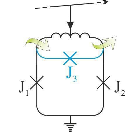
New superconducting reversible circuit for logical elements of the BISQUID supercomputer. J1, J2 - Josephson contacts, J3 (blue) - Josephson contact with a ferromagnet
The name "BSCVID" comes from the abbreviation "SQUID" (from the English SQUID - Superconducting Quantum Interference Device) - a superconducting quantum interference device with a unique sensitivity to a magnetic field. The prefix "bi" in the title reflects the unification of the functions of two SQUIDs in one scheme.
It is known that the high power consumption of modern supercomputers is a difficult problem on the way of their further development. According to the estimates of scientists, a further increase in productivity at the same pace as today will lead to the fact that the operation of one next-generation supercomputer will require a personal unit of a nuclear power plant.
“Energy consumption depends on a number of factors, including the principles of implementation of logical operations and the choice of materials used to create microchips,” Nikolai Klenov, associate professor at the Physics Department of Moscow State University, comments on the situation.
The processes occurring in all modern computers - personal and supercomputers, are irreversible. This means that some of the information in the process of calculation is lost, that is, according to the obtained result, we cannot recover what was at the input. This loss of information is accompanied by a loss of energy and an increase in the temperature of the computer, which was shown in 1961 in the work of R. Landauer. The use of semiconductor materials with electrical resistance, also leads to the fact that the calculations are accompanied by loss of energy and heating of the computer. For the computer to work, it is necessary not only to compensate for the loss of energy, but also to cool the chips to operating temperature. The natural way out of this situation can be the use of reversible logical operations that take place without loss of information, and the creation of computer chips using superconducting materials whose electrical resistance is zero.
By the way, recently, US and Japanese scientists experimentally showed that the power consumption of reversible superconducting circuits can be more than 6 orders of magnitude lower than the power consumption of existing semiconductor analogues, while the power consumption of existing digital superconducting electronics circuits is lower only by 3 order. But the superconducting circuits studied by them were rather cumbersome by the standards of modern nanotechnology, which prevents the creation of a supercomputer on their basis.
To solve the problem, the staff of the Laboratory of Physics of Nanostructures of the INP, MSU, headed by Mikhail Kupriyanov, together with colleagues from the Faculty of Physics of Moscow State University, started creating new superconducting reversible circuits. They recently developed a basic element of a supercomputer's memory cell, the so-called Josephson junction with a ferromagnetic material. This invention makes it possible to rely on the creation of a compact and energy-efficient superconducting memory, the absence of which is a significant obstacle to the practical application of the existing digital superconducting technology. However, the logical operations used in this technology are irreversible, and, consequently, the energy efficiency of the circuits is low.
In order to achieve a drastic reduction in energy consumption, this time scientists of the Institute for Nuclear Physics and the Faculty of Physics of Moscow State University proposed a new superconducting reversible scheme for the logical elements of a supercomputer. It consists of three Josephson contacts, one of which is the previously proposed contact with a ferromagnet.
“The use of ferromagnets in superconducting reversible circuits makes it possible to significantly simplify their design, reduce the size and ensure the adiabatic flow of the information processing process,” commented the invention the senior research associate of the INP MSU Igor Solovyov. “According to the degree of intensity of energy release, the processes occurring in modern computers and in our proposed scheme can be compared with the turbulent flow of a mountain river at numerous rapids and with the quiet, almost imperceptible in appearance, flow of a wide, deep river on a plain.”
It remains for scientists to test their invention experimentally. In the case of funding, laboratory tests may take place already this year.
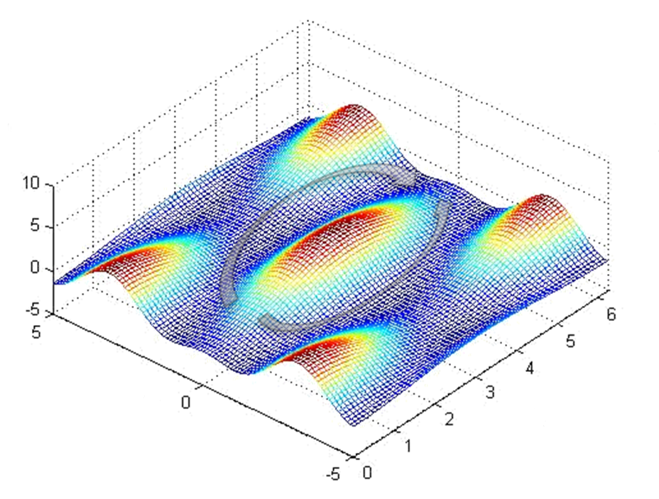
View of the constant component of the potential profile of a new reversible bi-SQUID scheme with a Josephson junction with a ferromagnet. The use of a ferromagnet ensures the existence of equipotential evolutionary trajectories of the system in the process of information transfer (shown by gray arrows), minimizing the energy release.
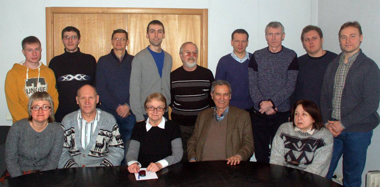
Top left to right: Alexey Zotovich, Sergey Zyryanov, Dmitry Lopaev, Dmitry Voloshin, Konstantin Klopovsky, Alexander Palov, Yuri Mankelevich, Konstantin Kurchikov, Alexander Chukalovsky Below from left to right: Olga Proshina, Alexander Kovalev, Tatyana Rakhimova, Alexander Rakhimov, Anna Vasilyeva
The group under the leadership of A.T.Rakhimov conducts research on the interaction of plasma with modern electronics materials with ultra-low dielectric constant. Details - in an interview with the leading researcher of the department of microelectronics of the INP, MSU, Candidate of Physical and Mathematical Sciences Dmitry Lopaev.
- Dmitry Viktorovich, tell us about your work in the group led by A.T. Rakhimov.
- We are working with new nanoporous materials with low dielectric constant (low-k films), which allow the distribution of signals in new chips with a high packing density of elements - the distance (half-pitch) between the elements of 10-22 nanometers. The smaller this distance, the more elements can be made on one square centimeter. We are now talking about a thousand billion items per square centimeter. These are processors, this is memory. In reality, these are such things, when you will have enormous computing power on one palm.
- How porous materials?
- Up to 50 percent porosity. It’s like cheese with lots of holes close to each other. The size of a typical nanopore is from 2 to 4 nanometers, that is, it is actually several layers of atoms. This porous material is very light, lighter than carbon CFRP, but it also has very high strength. Twice stronger than quartz. It resembles fluff or snow, but you will clear the snow, but it does not. It is durable, as it is bound. This material is pressed.
- What is the density?
- The density of modern low-k dielectrics of the order of and less than one gram per cubic centimeter.
- What are these materials and who produces them?
- All materials are provided by foreign partners. There are no such materials in Russia, as there is no production.
It is an organosilicate material consisting of silicon, oxygen, carbon, and hydrogen. And that's why SiOCH material is called. This is the most promising material.
- What is your contribution?
- We started working more than six years ago. The second was the generation of these materials, and the task was to implement the 22 technology nanometer, which are now used in the latest generation of processors from Intel. It is also solid-state drives, such terabyte drives of such size as your mobile phone.
Our contribution to technology is that we gain knowledge of how these materials are degraded in plasma under the conditions of the production process. That is how degradation mechanisms occur during etching. Knowing this, you can suggest ways to avoid degradation.
- What knowledge did you gain from degradation?
- The fact is that the material is very porous. If even a little water gets into the pores, the material will swallow it like a sponge and that's it, the dielectric material will not work. After all, water has a very high polarizability, and, therefore, there will be a high dielectric constant. Therefore, the material must be hydrophobic.
Hydrophobicity is achieved using CH3-methyl groups covering the entire inner surface of the pores. But, unfortunately, Si-CH3 groups are very susceptible to chemical reactions with active particles - ions, radicals, photons, which fall into the film from the plasma during the process. And here are the tasks: to understand what happens to the Si-CH3 groups under the action of the plasma; and how to ensure that they are not removed, because as soon as the CH3 groups are removed, water penetrates the pores and the material can be discarded as it degrades.
- And how to be?
- According to the principle, as in the “Caucasian Captive”: the one who disturbs us will help us. This principle was used in our scientific work; it turned out to be very vital.
- How is this possible, tell?
- It turned out that the same hard photons, but from a different plasma, from a noble helium plasma, which are strongly absorbed, they modify not only the surface, but also the internal structure of the SiO2 material. And the top layer of material is compressed. If ions are still bombarded, breaking bonds, a dense crust is formed, but very thin, only a few nanometers thick. And it turns out that we are sealing the material - and there is no degradation, because nothing already penetrates there. This was shown by us, and the technologists mastered it in production.
But, unfortunately, to avoid penetration of hard radiation into the film is impossible. They tried to cover from above, too, in layers, in a thin crust, but it is so thin that radiation still penetrates, and degradation goes even under this crust. And so we went to the cryogenic process. This is when you freeze at cryogenic temperature - minus 100 - some products in the pores and calmly make the structure. In this way, you do not let the radicals or anything else penetrate there, which leads to a defect. After that, you sublimate, by heating the material, remove the products from these pores, and it turns out that you made the structure, but did not spoil the neighboring section.
- What other material degradations are observed during the technological process?
- We need the architecture of the connection layer in the processor to be etched. But those radicals that poison, it usually occurs in fluorocarbon plasma, cause degradation: they remove the methyl groups, penetrating the pores. You are making a structure, you have etched everything, and everything that is near is already spoiled.
- What to do in this case?
- There are several ways. Right now, we are directly engaged in finding out how the etching mechanism itself, the degradation, already with fluorine atoms occurs. Already have an understanding. And it helps us a lot that the university has a lot of different equipment.
- What are the diagnosis?
- We have to do a lot of complex diagnostics: FTIR, RBS, XRF, XPS. Here XPS is the study of the surface with the help of radiation, when you knock electrons from the lower shells with hard photons, and transitions from the upper shells characterize the structure of the material. And, analyzing energy, you can understand, because you feel chemical shifts, its energy depends on the element and with which it is chemically bound. Analyzing these spectra, one can understand with the highest precision how atoms are bound on the surface. I want to say, in order to carry out only one spectroscopic ellipsometry, which has nanometer sensitivity, a whole complex of very complex diagnostics is needed. And doing it somewhere on the side is very expensive. Each diagnostic is thousands of dollars.
MSU is one of the few organizations in the world that can afford the luxury of doing such complex research and making hundreds of samples. We conduct advanced research, because we understand a lot in the study of modern plasma.
But still, we don’t get into development, that is, the development of specific things, it is closed to us, because this technology is not Russian. And you need to create your own development center. Otherwise we will not develop anything of our own.
Intellectual property rights remain with us. If we suddenly want to introduce some kind of technology, suddenly it will develop with us, we can apply what we have done without any licenses here.
We are one of the very few in Russia who are researching nanoporous materials. We are now a little shard. Russia needs a certain center. In such a center, such groups as ours should be a lot in different directions, but for them there should be a certain cube of clean rooms in which, as in a designer, I could put together different technologies. Not managers to collect, and technology, precisely when there are various devices, different technological lines. I could rent from some Western company, so we need non-profit agreements. Then it is possible to develop, and all that you have done is yours. We must have our own electronics.
Information